GITNUXSOFTWARE ADVICE
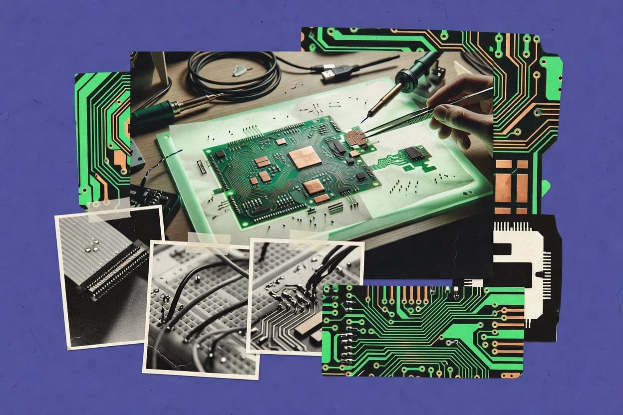
Manufacturing EngineeringTop 10 Best Circuit Maker Software of 2026
Top 10 Circuit Maker Software picks compared by features and pricing. Explore the best tools for PCB design, including Fusion 360, Altium, and KiCad.

How we ranked these tools
Core product claims cross-referenced against official documentation, changelogs, and independent technical reviews.
Analyzed video reviews and hundreds of written evaluations to capture real-world user experiences with each tool.
AI persona simulations modeled how different user types would experience each tool across common use cases and workflows.
Final rankings reviewed and approved by our editorial team with authority to override AI-generated scores based on domain expertise.
Score: Features 40% · Ease 30% · Value 30%
Gitnux may earn a commission through links on this page — this does not influence rankings. Editorial policy
Editor’s top 3 picks
Three quick recommendations before you dive into the full comparison below — each one leads on a different dimension.
Autodesk Fusion 360
Parametric CAD with linked assemblies for packaging electronics-ready mechanical designs
Built for hardware teams needing mechanical CAD plus manufacturable outputs for circuit builds.
Altium Designer
Editor pickConstraint-driven DRC with interactive routing integration across schematic and PCB domains
Built for professional PCB teams needing advanced constraint checking and fabrication-ready outputs.
KiCad
Editor pickDesign Rule Check with customizable net classes and DRC constraints
Built for engineers needing full schematic-to-PCB control without proprietary lock-in.
Related reading
Comparison Table
This comparison table benchmarks Circuit Maker Software against major design and PCB toolchains, including Autodesk Fusion 360, Altium Designer, KiCad, CADSTAR, EasyEDA, and other widely used alternatives. It summarizes the practical differences that affect everyday workflows such as schematic capture, PCB layout depth, component libraries, simulation and integration options, and export compatibility for downstream manufacturing.
Autodesk Fusion 360
PCB designProvides circuit board and electronic design workflows with schematic capture, PCB layout, simulation, and manufacturing data export.
Parametric CAD with linked assemblies for packaging electronics-ready mechanical designs
Autodesk Fusion 360 stands out for unifying CAD, CAM, and PCB-adjacent workflows around a single project model. Users can design and simulate enclosures and mechanical parts that pair with electronics workflows, then generate production-ready toolpaths through built-in CAM.
The platform also supports collaborative file management and model reuse, which benefits iterative prototype cycles for circuit-adjacent builds. Tight integration across modeling, manufacturing, and collaboration makes it useful beyond schematic-level tooling.
- +Integrated CAD with simulation and CAM in one project environment
- +Parametric modeling and reusable components speed repeated hardware revisions
- +Assembly workflows help package electronics with mechanical accuracy
- +Rich export options support downstream electronics and manufacturing steps
- –PCB-centric tasks are weaker than dedicated EDA tools
- –CAM setup and post processing require learning to get consistent outputs
- –Complex assemblies can slow performance on modest hardware
Best for: Hardware teams needing mechanical CAD plus manufacturable outputs for circuit builds
More related reading
Altium Designer
PCB designSupports schematic entry and high-performance PCB layout with rules-driven design, fabrication outputs, and production collaboration.
Constraint-driven DRC with interactive routing integration across schematic and PCB domains
Altium Designer stands out with its tight integration from schematic capture through PCB layout and manufacturing data creation. It supports advanced PCB workflows such as rigid-flex design, interactive routing, and constraint-driven rule checks.
Libraries, simulation hooks, and advanced design-for-manufacturability checks help teams manage complex electronic systems with fewer downstream surprises. The software is powerful for professional PCB engineering, but it brings a steep learning curve and heavy configuration overhead for small projects.
- +Deep schematic-to-PCB workflow with constraint-driven validation
- +Rigid-flex and advanced routing support complex board topologies
- +High-quality manufacturing outputs with robust DRC and fabrication checks
- +Powerful component and footprint management for large libraries
- –Dense interface and toolchain increase setup and learning time
- –Many advanced features require configuration discipline to stay consistent
- –Hardware resource demands can slow builds on midrange systems
Best for: Professional PCB teams needing advanced constraint checking and fabrication-ready outputs
KiCad
open-source EDADelivers open-source schematic capture and PCB layout with library management, DRC, and standard fabrication output generation.
Design Rule Check with customizable net classes and DRC constraints
KiCad stands out for being a complete open-source EDA suite covering schematic capture and PCB layout in a single workflow. It supports symbol and footprint libraries, design rule checks, and generation of fabrication outputs like Gerbers and drill files.
Advanced users get tight control over footprints, net classes, and rule-based constraints across the entire layout process. The toolchain remains fully file-based, which fits version control and long-lived project maintenance.
- +Integrated schematic capture, PCB layout, and DRC in one toolchain
- +Solid design rule checks with net classes and constraint-driven routing
- +Generates fabrication outputs like Gerbers and drill files for production-ready workflows
- +Extensive symbol and footprint library support with custom library creation
- –UI and workflows can feel dense for first-time PCB designers
- –Library and footprint quality varies, requiring careful verification per project
- –Hierarchical schematics and large projects need disciplined organization to stay manageable
Best for: Engineers needing full schematic-to-PCB control without proprietary lock-in
More related reading
CADSTAR
PCB designProvides PCB schematic and layout design with manufacturing data preparation for electronics manufacturing engineering workflows.
Integrated schematic-to-PCB connectivity with design rule checking and annotation propagation
CADSTAR from mentor.com stands out for circuit-centric drafting that connects schematic capture to rules-based PCB design workflows. It supports hierarchical schematics, multi-sheet projects, and structured component libraries to keep large electronics designs organized. The tool emphasizes design rule checking, connectivity management, and annotation flows that reduce board layout errors when changes propagate across documents.
- +Rules-driven PCB and DRC help catch connectivity and manufacturing issues early
- +Hierarchical schematic and multi-sheet organization supports complex electronics projects
- +Strong net and annotation workflows reduce rework when schematics change
- –Learning curve is steep for teams new to CADSTAR command workflows
- –Library and symbol setup can be time-consuming for custom component libraries
- –Depth of PCB automation features can feel overwhelming for small single-board work
Best for: Engineering teams needing schematic-to-PCB consistency with rigorous rule checking
EasyEDA
web-based EDAOffers browser-based schematic capture and PCB layout with online libraries and fabrication-ready output generation.
One-click conversion and reuse between schematics and PCB footprints through EasyEDA’s component library
EasyEDA focuses on browser-based schematic capture and PCB design with an integrated component library workflow. It supports hierarchical schematics, net and ERC checks, and PCB layout with autorouting and fabrication-ready outputs.
Collaboration and revision support appear through project sharing and cloud storage, which reduces local setup friction. Strong third-party part importing and footprint reuse help teams build circuits faster and maintain consistency across designs.
- +Browser-based schematic and PCB editing removes local toolchain friction
- +Integrated component library and footprint management speeds up new designs
- +ERC and design rule checks help catch net and layout issues early
- +Autorouter supports quicker initial board routing for common topologies
- +Gerber and manufacturing exports follow a fabrication-oriented workflow
- –Advanced CAD workflows can feel constrained versus desktop-grade editors
- –Complex constraint control and routing strategy tuning takes extra effort
- –Library coverage varies by part family and may require footprint cleanup
- –Documenting large multi-sheet projects can become cumbersome
Best for: Independent makers and small teams needing fast web-based circuit to PCB flow
EPLAN
electrical designCreates and manages electrical engineering schematics, panel design artifacts, and manufacturing documentation for production workflows.
Data-driven component and terminal management that keeps documentation consistent across the project
EPLAN stands out with deep electrical engineering orientation and document-driven workflows for large schematic and wiring projects. It supports schematic design, cable and terminal documentation, and consistent cross-referencing across design, harnessing, and equipment views.
Strong data management, rule-based structuring, and mature project templates help teams scale complex circuit documentation with fewer inconsistencies. Its primary focus aligns with industrial electrical documentation rather than casual circuit prototyping workflows.
- +Industrial-grade electrical documentation for schematics and wiring workflows
- +Consistent cross-referencing from component data through circuit and terminal records
- +Rule-driven structuring to reduce manual errors in large documents
- –Complex workflows require setup and disciplined data modeling
- –Less focused on rapid breadboard-style prototyping and hobby iterations
- –Learning curve is steep for teams without existing EPLAN conventions
Best for: Engineering teams producing industrial electrical schematics and wiring documentation at scale
More related reading
Zuken CR-8000
enterprise EDADelivers rules-driven electrical and PCB-centric design with large-project configuration management and manufacturing outputs.
Constraint-driven PCB layout with automated consistency checking across design data
Zuken CR-8000 stands out for automating schematic and PCB design with tight integration across the design flow. It supports multi-sheet schematics, rule-driven PCB layout, and constraint management that helps maintain electrical and physical consistency.
The environment also emphasizes library management and reuse for recurring product designs. For teams migrating legacy Zuken workflows, CR-8000 focuses on continuity while extending layout productivity through automated checking and consistency enforcement.
- +Rule-driven constraint management reduces electrical and layout inconsistencies
- +Automated design checks speed up DRC and connectivity validation cycles
- +Strong schematic-to-layout workflow supports complex multi-sheet projects
- +Reusable libraries improve throughput for recurring connector and harness designs
- –Dense configuration and rules can slow initial setup for new workflows
- –Learning curve increases when tailoring constraints to unique board practices
- –Workflow optimization depends on disciplined data management and library hygiene
Best for: Engineering teams needing rule-based schematic and PCB consistency at scale
Autodesk AutoCAD Electrical
electrical designProvides electrical schematic design with symbol libraries, wiring diagrams, and documentation workflows for manufacturing engineering.
Tag and wire number consistency via rule-based symbol and wire numbering tools
Autodesk AutoCAD Electrical stands out by automating electrical drawing tasks directly inside a CAD workflow, including symbol placement and wire number consistency. It supports schematic drafting with rule-based annotations, panel layouts, and project-wide drawing standard checks.
The software also includes report generation for bills of materials, cable schedules, and wire cross-references to reduce manual spreadsheet work. Circuit maker teams benefit most when large systems require consistent documentation across many drawings.
- +Rule-based wiring and tagging tools keep wire numbers and references consistent
- +Built-in electrical symbol libraries speed up drafting and reduce manual symbol errors
- +Project-level reports generate cable schedules, BOMs, and cross-references quickly
- +Panel and ladder workflow support reduces rework between schematic and build views
- +Drawing standard checks help catch missing tags and inconsistent identifiers
- –Configuration of project rules and templates can take significant upfront setup
- –Tooling feels CAD-centric, which slows teams wanting a pure circuit-first workflow
- –Complex custom symbol logic can be difficult to maintain over long projects
- –Large drawing sets can stress performance during intensive edits and batch updates
Best for: Electrical design teams needing consistent schematics, tagging, and documentation reports
More related reading
Capture
schematicsSupports schematic design and project management with electrical netlist handling for downstream PCB layout and manufacturing steps.
Rules-based schematic-to-PCB transfer that preserves net connectivity and design constraints
Capture in Altium focuses on turning schematics into manufacturable PCB data with tight integration to Altium’s PCB design workflow. It supports hierarchical schematics, libraries, symbol and footprint referencing, and rules-driven transfer into PCB layout. For Circuit Maker users, the distinct value is how consistently schematic intent can map into board constraints and design files without format handoffs.
- +Schematic-to-PCB handoff stays consistent with Altium’s constraint-driven workflow
- +Hierarchical schematics and libraries reduce repetition in larger designs
- +Rules and cross-references help catch schematic issues before board layout
- –Advanced electrical and project configuration can feel complex for casual work
- –Circuit Maker style workflows require extra discipline to avoid mismatched design intent
- –Library and rules management overhead grows on multi-project environments
Best for: Teams standardizing schematic-to-board workflows in an Altium-centric toolchain
Network Analyzer for PCB Design
prototypingGenerates board-level layouts from wiring diagrams and exports PCB artifacts for small-scale prototyping and production handoff.
Connectivity comparison that flags missing and mismatched net links between schematic intent and PCB
Network Analyzer for PCB Design stands out by focusing on automated connectivity checking for PCB layouts using netlist comparison workflows. It supports importing and analyzing design-rule relevant connectivity information to detect missing links, breaks, and mismatches between schematic intent and the PCB.
It also emphasizes visualization of connectivity results so issues can be traced back to specific nets and components. The tool’s core strength is targeted network validation rather than full circuit creation or schematic capture.
- +Detects net connectivity mismatches by comparing PCB links to intended net data
- +Highlights problematic nets and affected components for faster debugging
- +Fits PCB review workflows that need focused validation over full design automation
- –Best results depend on clean netlist and consistent net naming conventions
- –Limited coverage of broader ECAD tasks like routing optimization or full design editing
- –Connectivity reports can require manual interpretation for complex boards
Best for: PCB designers needing net connectivity validation and issue tracing
How to Choose the Right Circuit Maker Software
This buyer’s guide covers circuit maker software workflows across schematic capture, PCB layout, and production-ready outputs using tools like Autodesk Fusion 360, Altium Designer, KiCad, EasyEDA, and CADSTAR. It also maps industrial electrical documentation and project-driven wiring work using EPLAN and Autodesk AutoCAD Electrical. The guide explains what to look for, who each tool fits, and which mistakes to avoid across the full lineup of 10 tools.
What Is Circuit Maker Software?
Circuit maker software is application software that turns electrical or electronic design intent into manufacturable documentation and board-level artifacts. It typically includes schematic capture, electrical rule checks, PCB layout tools, and exports like Gerbers and drill files. Tools like Altium Designer and KiCad implement schematic-to-PCB workflows in a single toolchain with design-rule checking and fabrication outputs. CADSTAR and Capture focus on maintaining schematic connectivity and transferring that intent into PCB data so the board matches the schematic.
Key Features to Look For
The right feature set determines whether a tool prevents design errors early, produces outputs that manufacturing can use, and scales beyond a single board.
Constraint-driven design rule checking across schematic and PCB
Constraint-driven DRC reduces electrical and layout mistakes by validating connectivity and design rules during the workflow. Altium Designer delivers constraint-driven DRC with interactive routing integration across schematic and PCB domains, and KiCad provides customizable net classes with DRC constraints. CADSTAR supports rules-driven PCB design and design rule checking tied to connectivity and annotation flows.
Schematic-to-PCB transfer that preserves net connectivity
Schematic-to-PCB transfer matters when layout must reflect schematic intent without manual rebuilding of constraints or nets. Capture emphasizes rules-based schematic-to-PCB transfer that preserves net connectivity and design constraints. Network Analyzer for PCB Design complements this by checking connectivity mismatches between schematic intent and PCB links and highlighting problematic nets and components.
Library and footprint management for reliable reuse
Library quality directly affects connector, footprint, and symbol consistency across repeated revisions. Altium Designer is strong for component and footprint management in large libraries. EasyEDA adds fast reuse by enabling one-click conversion and reuse between schematics and PCB footprints through its component library workflow.
Advanced PCB topology handling and routing productivity
Routing productivity and topology support decide whether complex boards become hard to iterate. Altium Designer supports rigid-flex design and interactive routing, and EasyEDA includes autorouting for quicker initial board routing. Zuken CR-8000 adds constraint-driven PCB layout and automated consistency checking to keep complex design data aligned across revisions.
Manufacturing-ready fabrication outputs and production exports
Manufacturing-ready outputs reduce handoff work by generating the exact artifact types needed for fabrication. KiCad generates fabrication outputs like Gerbers and drill files. EasyEDA follows a fabrication-oriented workflow with Gerber and manufacturing exports, and Altium Designer provides robust fabrication outputs with DRC and fabrication checks.
Documentation and data management for large electrical projects
For wiring and panel documentation, circuit maker tools must manage component, terminal, and reference data across many documents. EPLAN delivers data-driven component and terminal management that keeps documentation consistent across the project. Autodesk AutoCAD Electrical automates wiring and tagging with rule-based symbol and wire numbering and generates project-level reports for BOMs and cable schedules.
How to Choose the Right Circuit Maker Software
Choosing the right tool starts with matching the workflow target and error-prevention needs to the capabilities of specific ECAD or electrical documentation platforms.
Match the tool to the core output goal: PCB fabrication, validation, or industrial documentation
Teams focused on professional PCB engineering should evaluate Altium Designer because it combines schematic capture with constraint-driven DRC, advanced routing, and fabrication-ready outputs. Engineers prioritizing open workflow control and standard exports should evaluate KiCad because it integrates schematic capture, PCB layout, and DRC while generating Gerbers and drill files. Teams needing targeted connectivity validation can pair a primary ECAD workflow with Network Analyzer for PCB Design to flag missing and mismatched net links.
Verify that the connectivity story stays consistent from schematic intent to PCB reality
If net connectivity preservation is the priority, Capture provides rules-based schematic-to-PCB transfer that preserves net connectivity and design constraints within an Altium-centric chain. CADSTAR helps enforce consistency through integrated schematic-to-PCB connectivity with design rule checking and annotation propagation. Network Analyzer for PCB Design adds a separate connectivity comparison step that detects breaks between schematic intent and the PCB layout.
Choose a rule-checking approach that fits the complexity of the designs and the team’s discipline
Altium Designer excels when constraint-driven validation and interactive routing are required for complex board topologies like rigid-flex. KiCad supports DRC through customizable net classes and DRC constraints, which benefits engineers who want explicit control over rule behavior. Zuken CR-8000 focuses on constraint-driven PCB layout with automated consistency checking and is designed for rule-based continuity across design data.
Assess CAD and mechanical packaging needs before assuming the toolchain can cover everything
Hardware teams that need mechanical packaging linked to electronics workflows should evaluate Autodesk Fusion 360 because it provides parametric CAD with linked assemblies for packaging electronics-ready mechanical designs and supports circuit-adjacent outputs. For pure electrical schematic and PCB execution without heavy mechanical workflows, KiCad and Altium Designer tend to fit better because their strengths center on schematic-to-PCB editing and fabrication output generation.
Pick the environment that best matches how the team works: web, desktop, or document-driven industrial systems
Makers and small teams that want a browser-based workflow should evaluate EasyEDA because it enables browser-based schematic and PCB editing with integrated component library workflow and autorouting. Industrial engineering teams producing wiring and terminal documentation at scale should evaluate EPLAN because it uses data-driven component and terminal management with rule-driven structuring. Electrical teams needing consistent schematics plus wire numbering, symbol libraries, and report generation should evaluate Autodesk AutoCAD Electrical because it automates tag and wire number consistency with rule-based symbol and wire numbering tools.
Who Needs Circuit Maker Software?
Circuit maker software fits different roles depending on whether the work centers on PCB design, connectivity validation, electrical documentation, or mechanical-electrical packaging.
Hardware teams that need mechanical packaging plus manufacturable electronics outputs
Autodesk Fusion 360 is the best fit for hardware teams because it combines parametric CAD and simulation with electronics workflow integration and supports packaging electronics-ready mechanical designs. Fusion 360 also supports collaborative file management and reusable components that speed repeated hardware revisions.
Professional PCB teams building complex board topologies and requiring advanced constraint checking
Altium Designer fits professional PCB teams because it provides constraint-driven DRC with interactive routing integration and supports rigid-flex design and high-performance PCB layout. Zuken CR-8000 also targets engineering teams that need rule-based schematic and PCB consistency at scale through constraint-driven PCB layout and automated design checks.
Engineers who want full schematic-to-PCB control without proprietary lock-in
KiCad fits engineers needing open-source schematic capture and PCB layout with integrated DRC and standard fabrication output generation. KiCad’s customizable net classes support constraint-driven validation during layout while generating production artifacts like Gerbers and drill files.
Independent makers and small teams needing fast web-based circuit to PCB flow
EasyEDA fits independent makers and small teams because it is browser-based and includes integrated component library workflow, ERC, and design rule checks. EasyEDA also supports autorouting for quicker initial board routing and follows a fabrication-oriented workflow with Gerber and manufacturing exports.
Common Mistakes to Avoid
Missteps usually come from picking a tool that does not match the workflow boundary, skipping rule-check discipline, or allowing library and net naming quality to degrade.
Assuming PCB-centric tools handle mechanical packaging without a real CAD link
Fusion work requires explicit assembly and packaging design, so Autodesk Fusion 360 is the right option when parametric CAD with linked assemblies is needed for electronics-ready mechanical designs. Tools centered on schematic-to-PCB execution like KiCad and Altium Designer focus on electrical artifacts and can leave mechanical packaging to separate CAD workflows.
Skipping connectivity validation after schematic-to-board transfers
Network Analyzer for PCB Design helps prevent undetected mismatches by comparing PCB links to intended net data and highlighting problematic nets and affected components. Capture and CADSTAR reduce connectivity mistakes through rules-based schematic-to-PCB transfer and integrated schematic-to-PCB connectivity with annotation propagation.
Building on weak component and footprint libraries without verification
Library and footprint quality can vary, which makes verification necessary in KiCad when creating or maintaining symbol and footprint libraries. Altium Designer and EasyEDA reduce rework through deep component and footprint management with library reuse, including EasyEDA’s one-click conversion and reuse between schematics and PCB footprints.
Using a powerful constraint system but not configuring it in a disciplined way
CADSTAR and Zuken CR-8000 rely on rules-driven workflows where setup and command discipline affect throughput, so teams need clear constraint and library hygiene. Altium Designer also provides dense constraint capabilities, so staying consistent requires intentional configuration for each project.
How We Selected and Ranked These Tools
we evaluated every tool using three sub-dimensions: features with a weight of 0.4, ease of use with a weight of 0.3, and value with a weight of 0.3. The overall rating is the weighted average of those three sub-dimensions using overall = 0.40 × features + 0.30 × ease of use + 0.30 × value. Autodesk Fusion 360 separated itself from lower-ranked tools by combining integrated CAD with simulation and CAM features at the project level, which supports real manufacturable packaging outcomes and strengthened the features dimension for hardware teams. That integrated workflow also helped deliver practical end-to-end outputs, which improved how the tool’s feature set connected to real deliverables rather than stopping at schematic or layout stages.
Frequently Asked Questions About Circuit Maker Software
Which toolchain best supports schematic-to-PCB consistency for circuit maker projects?
What option provides the most automated connectivity validation when PCB layout changes after schematic capture?
Which circuit maker software is best for teams that need advanced PCB constraint checking beyond basic design rule checks?
Which tool is most suitable for circuit makers who want full control over footprints, net classes, and file-based project maintenance?
Which software best fits projects that include mechanical packaging and enclosure design alongside circuit work?
Which option is most practical for building circuits quickly in a browser-based workflow?
Which tool is aimed at large industrial electrical documentation rather than prototyping circuits?
What software helps reduce errors when wiring and tagging must remain consistent across many drawings?
Which circuit maker tool is strongest for migrating or extending existing Zuken-based design workflows?
Conclusion
After evaluating 10 manufacturing engineering, Autodesk Fusion 360 stands out as our overall top pick — it scored highest across our combined criteria of features, ease of use, and value, which is why it sits at #1 in the rankings above.
Use the comparison table and detailed reviews above to validate the fit against your own requirements before committing to a tool.
Tools reviewed
Primary sources checked during evaluation.
Referenced in the comparison table and product reviews above.
Keep exploring
Comparing two specific tools?
Software Alternatives
See head-to-head software comparisons with feature breakdowns, pricing, and our recommendation for each use case.
Explore software alternatives→In this category
Manufacturing Engineering alternatives
See side-by-side comparisons of manufacturing engineering tools and pick the right one for your stack.
Compare manufacturing engineering tools→FOR SOFTWARE VENDORS
Not on this list? Let’s fix that.
Our best-of pages are how many teams discover and compare tools in this space. If you think your product belongs in this lineup, we’d like to hear from you—we’ll walk you through fit and what an editorial entry looks like.
Apply for a ListingWHAT THIS INCLUDES
Where buyers compare
Readers come to these pages to shortlist software—your product shows up in that moment, not in a random sidebar.
Editorial write-up
We describe your product in our own words and check the facts before anything goes live.
On-page brand presence
You appear in the roundup the same way as other tools we cover: name, positioning, and a clear next step for readers who want to learn more.
Kept up to date
We refresh lists on a regular rhythm so the category page stays useful as products and pricing change.