GITNUXSOFTWARE ADVICE
Manufacturing EngineeringTop 8 Best Electronic Board Design Software of 2026
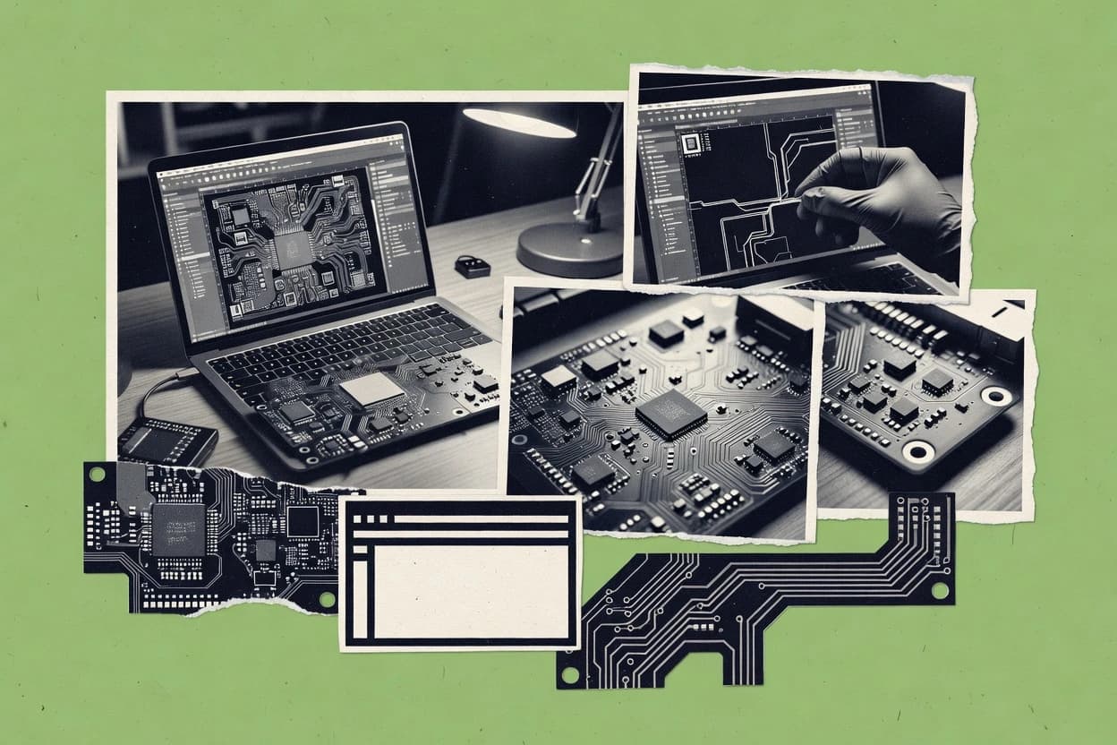
Top 10 Electronic Board Design Software rankings. Compare Altium Designer, Autodesk EAGLE, KiCad and other picks for PCB design workflows.

How we ranked these tools
Core product claims cross-referenced against official documentation, changelogs, and independent technical reviews.
Analyzed video reviews and hundreds of written evaluations to capture real-world user experiences with each tool.
AI persona simulations modeled how different user types would experience each tool across common use cases and workflows.
Final rankings reviewed and approved by our editorial team with authority to override AI-generated scores based on domain expertise.
Score: Features 40% · Ease 30% · Value 30%
Gitnux may earn a commission through links on this page — this does not influence rankings. Editorial policy
Editor’s top 3 picks
Three quick recommendations before you dive into the full comparison below — each one leads on a different dimension.
Altium Designer
Integrated constraint-driven design with advanced signal-integrity and high-speed analysis
Built for teams building complex, high-speed PCBs needing tight constraint control.
Autodesk EAGLE
Editor pickERC and DRC rule checks that validate schematics and PCB constraints before CAM export
Built for teams needing reliable PCB layout and manufacturable outputs for common board types.
KiCad
Editor pick3D PCB viewer with interactive rendering of footprints and board outline
Built for teams needing deterministic, scriptable PCB design without proprietary lock-in.
Related reading
Comparison Table
This comparison table reviews electronic board design software used for schematic capture, PCB layout, and manufacturing output generation. It contrasts tools such as Altium Designer, Autodesk EAGLE, KiCad, Cadence OrCAD PCB Designer, and Mentor Graphics PADS across core capabilities and practical workflow differences. Readers can map each package to expected design needs, from library management and constraint handling to file handoff for fabrication.
Altium Designer
Pro CADAltium Designer provides schematic capture and PCB layout with rule-based design, interactive routing, and integrated library workflows for manufacturing-ready electronic boards.
Integrated constraint-driven design with advanced signal-integrity and high-speed analysis
Altium Designer stands out with a highly integrated PCB design environment that tightly links schematic capture, PCB layout, and rules-driven design checking. It supports advanced constraint management, including net and component constraints, for controlling routing, clearances, and fabrication-ready stackups.
The tool includes simulation and signal integrity workflows, which help validate high-speed designs before release. Collaboration features like version-controlled project management help teams coordinate changes across complex board families.
- +Rules-driven PCB layout with strong constraint management
- +Tightly integrated schematic-to-layout workflow with net consistency
- +High-speed and signal-integrity tools for pre-release validation
- +Flexible stackup and fabrication outputs for board houses
- –Complex setup can slow early projects and onboarding
- –Resource-heavy on large designs requiring robust workstation specs
- –Deep toolchain integration increases configuration and workflow overhead
Best for: Teams building complex, high-speed PCBs needing tight constraint control
More related reading
Autodesk EAGLE
PCB CADAutodesk EAGLE delivers schematic entry and PCB layout with component libraries, electrical rules checks, and export flows geared toward fabrication output.
ERC and DRC rule checks that validate schematics and PCB constraints before CAM export
Autodesk EAGLE stands out with its long-established schematic and PCB workflow plus a component library ecosystem built around EAGLE formats. It supports hierarchical schematics, net and ERC checks, and detailed PCB layout with routing, layers, and rule-based design validation.
The CAM output pipeline can generate manufacturing files from board data and design constraints. Its tight integration with Autodesk tooling helps teams move from capture to fabrication-ready deliverables with consistent project artifacts.
- +Fast schematic capture with hierarchical design and connectivity consistency checks
- +Rule-based PCB design checks including clearances, widths, and constraint enforcement
- +Integrated autorouting with interactive manual routing across configurable layers
- +Board and schematic linking keeps net names and references synchronized
- +CAM generation workflow produces fabrication outputs from layout data
- –EAGLE scripting and automation feel less approachable than modern plugin ecosystems
- –3D visualization and mechanical integration are limited compared with dedicated MCAD tools
- –Large multi-board projects can feel slower than newer stack-based CAD tools
Best for: Teams needing reliable PCB layout and manufacturable outputs for common board types
KiCad
Open-sourceKiCad offers open-source schematic capture and PCB layout with DRC support, 3D visualization, and fabrication export for board production.
3D PCB viewer with interactive rendering of footprints and board outline
KiCad stands out by combining schematic capture and PCB layout in one open-source toolchain with a consistent project format. It supports hierarchical sheets, ERC checks, and footprint management for accurate component-to-board mapping.
For PCB design, it includes interactive routing, design-rule checks, solid and interactive 3D previews, and Gerber and drill export for fabrication. It also integrates with scripting and file formats that fit automated workflows for netlists, footprints, and manufacturing outputs.
- +Unified schematic and PCB workflow with shared net and footprint data
- +Hierarchical schematics with electrical-rule checks for connectivity accuracy
- +Design-rule checking catches clearance, width, and constraint violations
- +Interactive routing supports constraints like track width and vias
- +3D viewer helps verify component height and mechanical placement
- +Outputs industry-standard Gerber and drill files for fabrication
- –Complex projects can feel slower during annotation and DRC cycles
- –Advanced impedance and stackup features require careful manual setup
- –Library quality depends on external footprint and symbol curation
- –CAM setup for specialized fabrication workflows can be time-consuming
Best for: Teams needing deterministic, scriptable PCB design without proprietary lock-in
Cadence OrCAD PCB Designer
EDA suiteOrCAD PCB Designer supports schematic-to-PCB workflows, constraint-driven placement and routing, and deliverables generation for printed circuit manufacturing.
Constraint-driven rule checking and DRC integrated into the PCB layout workflow
Cadence OrCAD PCB Designer stands out for its deep integration with Allegro-driven flows and Cadence toolchains used in professional hardware teams. It provides a complete schematic capture to PCB layout workflow with constraint management, rule-based design checking, and detailed routing tools.
The software supports signal-integrity aware placement and routing with typical fabrication outputs for manufacturing collaboration. Verification and documentation capabilities help reduce layout-to-design-cycle rework when iterating revisions across boards.
- +Tight toolchain integration for schematic and PCB handoff consistency
- +Rule-based DRC catches clearance and constraint violations early
- +Strong routing and constraint management for complex multi-net boards
- +Manufacturing-ready outputs for fabrication and assembly workflows
- +Verification tools support iterative layout refinement cycles
- –Learning curve is steep compared with entry-level PCB editors
- –Performance can degrade on very large designs with dense routing
- –Workflow complexity increases for teams with mixed tool ecosystems
- –Less ideal for lightweight prototyping-only use cases
- –Customization of flows can require significant setup effort
Best for: Professional PCB teams needing constraint-driven layout with strong verification
Mentor Graphics PADS
Professional PCBPADS provides schematic and PCB layout tools with connectivity-based design, DRC, and manufacturing deliverables support for multi-board projects.
Rule-driven PCB design checks that enforce clearances, connectivity, and footprint compliance
Mentor Graphics PADS stands out for integrating schematic capture with PCB layout inside a consistent design environment. The tool supports mixed-signal workflows, rule-driven design checks, and constraint-based routing to reduce rework on complex boards.
Component libraries and footprint management streamline reuse across product variants. The software also includes manufacturing handoff data generation for fabrication and assembly packages.
- +Constraint-driven routing supports controlled stackups and design rules
- +Tight schematic-to-PCA integration reduces cross-tool translation issues
- +Rule checks catch clearance and footprint violations early
- +Manufacturing output generation supports fabrication and assembly deliverables
- –Library and footprint setup requires careful standardization to stay consistent
- –Advanced flow tuning can feel rigid on highly customized processes
- –Large designs may demand significant workstation resources for smooth editing
Best for: Teams designing complex PCB layouts needing strong rule checking and handoff outputs
Siemens Xpedition
EDA enterpriseXpedition supports schematic and PCB design flows with constraint management and fabrication deliverables for printed circuit development.
Integrated rule-checking that enforces schematic-to-layout constraints during design closure
Siemens Xpedition stands out for deep, standards-driven board design flows integrated with Siemens EDA methodology. Core capabilities include schematic capture, hierarchical net management, and PCB layout with rule-driven constraint checking.
The tool supports simulation handoff workflows and robust connectivity verification so routing and fabrication constraints stay consistent. Xpedition is positioned for teams needing repeatable design closure across complex electronic assemblies.
- +Rule-based design checks catch violations during schematic-to-layout iteration
- +Strong hierarchical connectivity handling for large multi-sheet designs
- +Layout supports constraint-driven routing and consistent fabrication readiness
- +Verification tooling improves net, connectivity, and design closure confidence
- –Complex workflows can slow productivity for small single-board projects
- –Setup of design rules and constraints requires experienced administrators
- –Advanced integration features may demand tight IT environment control
- –Interface density increases learning effort compared with lightweight editors
Best for: Large teams needing rigorous design closure across complex PCB assemblies
ExpressPCB
Web-based CADExpressPCB offers web-based schematic and PCB layout with fabrication-ready outputs for board creation and quick manufacturing turnaround.
Schematic-to-layout workflow that streamlines getting PCBs ready for fabrication
ExpressPCB stands out for turning schematic-driven design into fabrication-ready PCB layouts without a heavy feature maze. It provides a guided workflow that supports board layout, routing, and generation of industry-standard manufacturing outputs.
The tool focuses on practical layout needs such as placing components, defining traces, and preparing files for PCB fabrication. It is best suited for users who want fast turnaround from drawing to production data.
- +Schematic-to-PCB workflow reduces manual translation work
- +Generates fabrication-ready output files for PCB production
- +Straightforward layout and routing tools for quick board creation
- –Limited depth for advanced layout automation and optimization
- –Less suited for complex high-density board design workflows
- –Fewer analysis and signal-integrity tools than specialized suites
Best for: Users needing quick PCB layout to manufacturing outputs
Fritzing
Prototype CADFritzing provides an electronics prototyping tool with schematic and PCB views and export paths for small board manufacturing workflows.
Breadboard to schematic to PCB view synchronization
Fritzing stands out for turning breadboard-style tinkering into a shareable electronic design workflow. It supports schematic, breadboard, and PCB layout views with component libraries and Arduino-friendly workflows.
Board files can be exported for manufacturing and shared for collaboration through a project-centric design format. The tool emphasizes rapid prototyping rather than rigorous electronics constraints management.
- +Three synchronized views link breadboard, schematic, and PCB layouts.
- +Large component library includes many common through-hole and header parts.
- +Exports PCB artwork suitable for basic fabrication workflows.
- –Design rule checking is limited for complex, constraint-heavy projects.
- –Net and connectivity errors can slip through without advanced validation.
- –PCB routing tools are less capable than professional CAD suites.
Best for: Hobbyists and educators prototyping circuits with visual board workflows
How to Choose the Right Electronic Board Design Software
This buyer's guide explains how to choose electronic board design software for schematic capture, PCB layout, and fabrication-ready output workflows using tools like Altium Designer, Autodesk EAGLE, KiCad, Cadence OrCAD PCB Designer, and Siemens Xpedition. It also covers workflow fit for Mentor Graphics PADS, ExpressPCB, and Fritzing, which emphasize different levels of automation and constraint checking.
What Is Electronic Board Design Software?
Electronic board design software combines schematic capture, PCB layout, and rule checking to produce fabrication outputs like Gerber and drill files or board manufacturing deliverables. It solves connectivity and constraint errors by linking nets from schematic to layout and enforcing rules such as clearances, widths, and fabrication stackups. Tools like Altium Designer connect schematic-to-layout with rule-driven design checking, while KiCad provides open-source schematic and PCB tools with DRC and Gerber and drill export for board production.
Key Features to Look For
These features determine whether a tool can move designs from schematic intent to manufacturing-ready PCBs with minimal rework.
Integrated constraint-driven design with schematic-to-layout net consistency
Altium Designer enforces constraints during rule-based PCB layout and keeps net relationships consistent from schematic capture into layout so routing follows design intent. Cadence OrCAD PCB Designer and Siemens Xpedition also integrate constraint-driven rule checking into the layout workflow to reduce layout-to-design-cycle rework.
ERC and DRC rule checks tied to fabrication-ready outcomes
Autodesk EAGLE validates schematics with ERC and validates PCB constraints with DRC before CAM export so manufacturing files reflect the routed design. Mentor Graphics PADS and Altium Designer enforce clearances, footprint compliance, and connectivity rules early to prevent downstream fabrication issues.
Signal integrity and high-speed analysis workflows
Altium Designer includes simulation and signal integrity workflows that help validate high-speed designs before release. This capability is paired with integrated constraint management, which matters when impedance control and high-speed routing constraints must stay aligned from design rules to layout.
Deterministic schematic and PCB data management for repeatable projects
KiCad offers a consistent open-source project format with hierarchical schematics and shared net and footprint data, which supports deterministic workflows. Siemens Xpedition adds rigorous hierarchical connectivity handling for large multi-sheet designs to maintain design closure across complex assemblies.
3D visualization for mechanical fit and footprint height verification
KiCad includes a 3D PCB viewer that renders footprints and the board outline with interactive 3D previews. Fritzing also synchronizes breadboard, schematic, and PCB views to help visualize placement, but KiCad provides the board-level mechanical verification path.
Fabrication output generation for board houses and assembly handoff
Autodesk EAGLE uses a CAM generation workflow that produces fabrication outputs from layout data, which supports consistent project artifacts. ExpressPCB and Fritzing generate fabrication-ready output files suitable for basic board production workflows, while Altium Designer, OrCAD PCB Designer, and Mentor Graphics PADS support manufacturing and assembly deliverables for complex product variants.
How to Choose the Right Electronic Board Design Software
The choice depends on how strict the design rules must be, how complex the board is, and how fast the workflow must turn schematic intent into manufacturing deliverables.
Start with the design strictness level needed for routing and constraints
For high-speed PCBs that require tight constraint control, Altium Designer is built around integrated constraint-driven PCB layout and advanced signal integrity validation. For professional teams that need DRC enforced in the layout workflow, Cadence OrCAD PCB Designer and Mentor Graphics PADS provide constraint-driven rule checking and manufacturing-ready handoff outputs.
Verify schematic capture quality through ERC and DRC before fabrication output
If schematic correctness must be validated with electrical rules before CAM export, Autodesk EAGLE pairs ERC and DRC rule checks with a CAM output pipeline. Siemens Xpedition also supports integrated rule checking that enforces schematic-to-layout constraints during design closure, which reduces the chance of producing inconsistent manufacturing data.
Match workflow speed to project size and team setup tolerance
If the organization can invest in complex setup for sophisticated rules and high-speed validation, Altium Designer fits teams that run large, dense designs on robust workstations. If faster guided layout is the priority for simpler boards, ExpressPCB focuses on a schematic-to-PCB workflow that generates fabrication-ready output files with a less complex feature maze.
Confirm mechanical and layout visualization for component fit risk
When component height and mechanical placement must be checked inside the design tool, KiCad uses an interactive 3D PCB viewer for board outline and footprint visualization. For rapid education and breadboard-style prototyping visualization, Fritzing synchronizes breadboard, schematic, and PCB views but does not provide the same advanced impedance and stackup support as professional PCB editors.
Select the right fabrication and manufacturing handoff depth
For teams that need rich manufacturing and assembly deliverables with strong constraint compliance, Mentor Graphics PADS and Cadence OrCAD PCB Designer support manufacturing output generation tied to rule-driven checks. For teams that prioritize industry-standard board files without proprietary lock-in, KiCad exports Gerber and drill files for fabrication using the project’s deterministic schematic and footprint data.
Who Needs Electronic Board Design Software?
Different electronic board design software tools fit different board complexity levels, verification requirements, and automation expectations.
Complex high-speed PCB teams that need advanced validation and constraint control
Altium Designer is the best match for teams building complex, high-speed PCBs because it combines rules-driven PCB layout with integrated simulation, signal integrity workflows, and advanced constraint management for fabrication-ready stackups.
Teams that must produce consistent manufacturing deliverables for common board types
Autodesk EAGLE fits teams that need reliable PCB layout with ERC and DRC rule checks and CAM generation for fabrication outputs, which helps keep project artifacts consistent from layout to manufacturing files.
Teams that want deterministic open-source workflows and strong board-level export formats
KiCad serves teams that want scriptable, deterministic PCB design without proprietary lock-in because it provides hierarchical schematics with ERC checks, DRC enforcement, interactive routing, and Gerber and drill export.
Professional PCB teams that require constraint-driven DRC in the layout workflow
Cadence OrCAD PCB Designer and Mentor Graphics PADS target professional teams that need rule checking to catch clearance, connectivity, and footprint compliance issues during layout and then generate manufacturing and assembly handoff data.
Common Mistakes to Avoid
The most common failures come from underestimating rule enforcement, library setup effort, or the workflow depth required for the target board complexity.
Ignoring constraint rigor until late in the layout cycle
Boards built with minimal DRC enforcement often discover clearance and constraint violations late, which is exactly what Autodesk EAGLE, Cadence OrCAD PCB Designer, and Mentor Graphics PADS are designed to prevent by running ERC and DRC checks before CAM export or handoff.
Choosing a tool that cannot close high-speed validation gaps
High-speed work can suffer if only basic layout and routing are used, which is why Altium Designer includes simulation and signal integrity workflows paired with constraint-driven design checking for pre-release validation.
Underestimating library and footprint quality effort
KiCad and Mentor Graphics PADS depend on footprint and library standardization quality, and poor footprint curation can cause connectivity and assembly mistakes even when DRC exists. Altium Designer reduces some translation issues with integrated library workflows, but any environment still requires footprint accuracy for manufacturing.
Using visualization features that do not match mechanical risk tolerance
Fritzing provides synchronized breadboard, schematic, and PCB views for rapid prototyping, but it offers limited design rule checking for complex constraint-heavy projects. KiCad’s interactive 3D PCB viewer better addresses mechanical placement and component height verification needs for production boards.
How We Selected and Ranked These Tools
We evaluated every tool on three sub-dimensions. Features received a weight of 0.4, ease of use received a weight of 0.3, and value received a weight of 0.3. The overall rating equals 0.40 × features + 0.30 × ease of use + 0.30 × value. Altium Designer separated itself by combining rules-driven PCB layout with integrated constraint management and advanced signal integrity workflows, which delivered very high feature capability while maintaining strong usability and value across complex high-speed PCB work.
Frequently Asked Questions About Electronic Board Design Software
Which electronic board design software keeps constraints consistent from schematic capture through PCB routing and fabrication checks?
Which toolchain is best for high-speed PCB work that needs signal integrity validation before release?
How do the open-source and scriptable workflows compare for automated PCB design tasks?
Which software produces manufacturable CAM outputs with strong connectivity and design-rule checks?
What options exist for multi-board collaboration and version-controlled project management?
Which tool is most appropriate for designing complex mixed-signal boards with enforced clearances and footprint compliance?
Which software fits professionals who already use Cadence and Allegro verification and layout flows?
How does guided schematic-to-PCB workflow differ from full-feature constraint-driven design environments?
What are the most practical options for teaching, prototyping, and sharing circuit layouts with visual views?
Conclusion
After evaluating 8 manufacturing engineering, Altium Designer stands out as our overall top pick — it scored highest across our combined criteria of features, ease of use, and value, which is why it sits at #1 in the rankings above.
Use the comparison table and detailed reviews above to validate the fit against your own requirements before committing to a tool.
Tools reviewed
Primary sources checked during evaluation.
Referenced in the comparison table and product reviews above.
Keep exploring
Comparing two specific tools?
Software Alternatives
See head-to-head software comparisons with feature breakdowns, pricing, and our recommendation for each use case.
Explore software alternatives→In this category
Manufacturing Engineering alternatives
See side-by-side comparisons of manufacturing engineering tools and pick the right one for your stack.
Compare manufacturing engineering tools→FOR SOFTWARE VENDORS
Not on this list? Let’s fix that.
Our best-of pages are how many teams discover and compare tools in this space. If you think your product belongs in this lineup, we’d like to hear from you—we’ll walk you through fit and what an editorial entry looks like.
Apply for a ListingWHAT THIS INCLUDES
Where buyers compare
Readers come to these pages to shortlist software—your product shows up in that moment, not in a random sidebar.
Editorial write-up
We describe your product in our own words and check the facts before anything goes live.
On-page brand presence
You appear in the roundup the same way as other tools we cover: name, positioning, and a clear next step for readers who want to learn more.
Kept up to date
We refresh lists on a regular rhythm so the category page stays useful as products and pricing change.