GITNUXSOFTWARE ADVICE
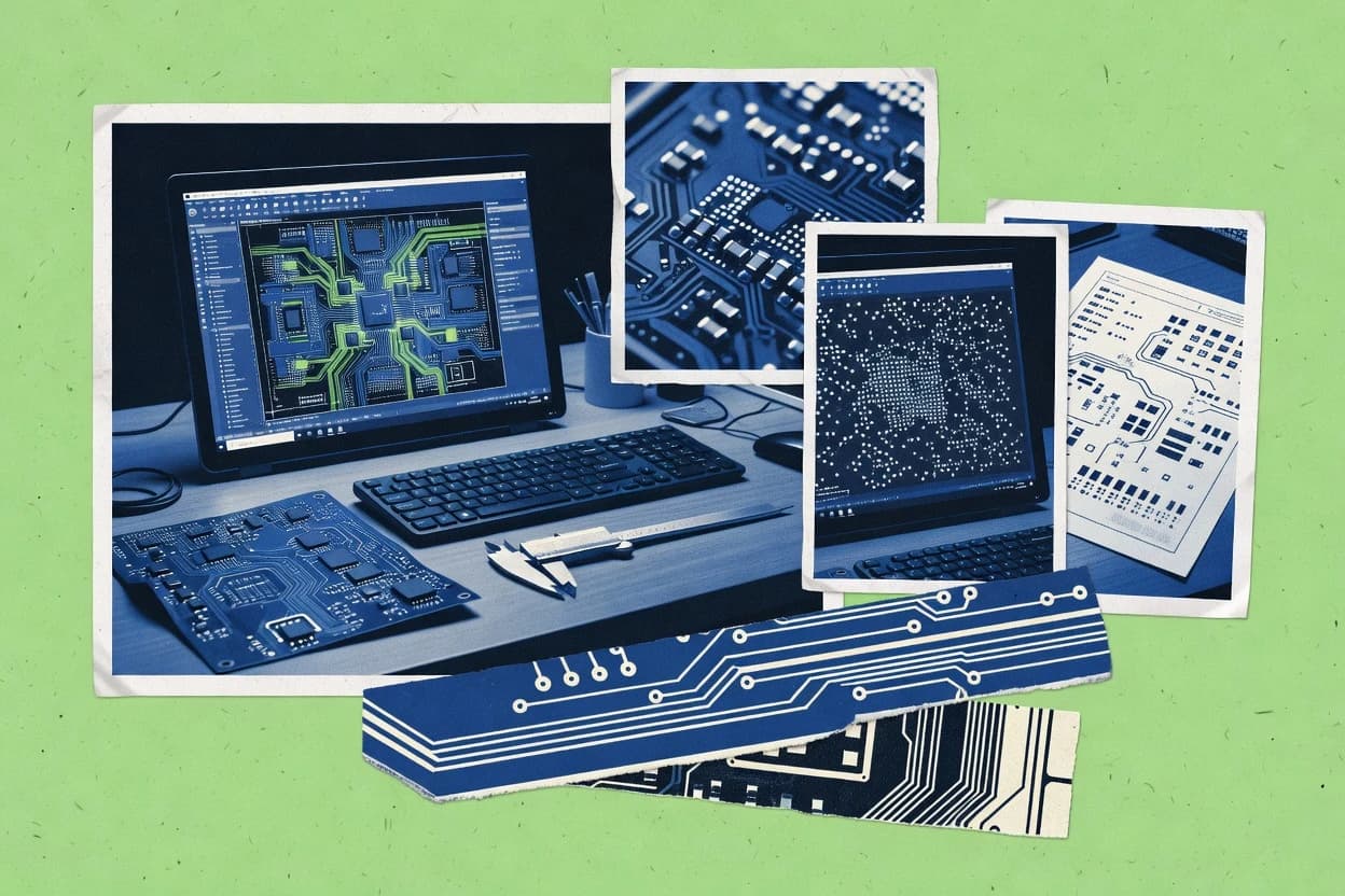
Manufacturing EngineeringTop 8 Best Electronic Cad Software of 2026
Top 10 Best Electronic Cad Software. Compare picks like Altium Designer, Autodesk EAGLE, and KiCad. Explore rankings and choose the right tool.

How we ranked these tools
Core product claims cross-referenced against official documentation, changelogs, and independent technical reviews.
Analyzed video reviews and hundreds of written evaluations to capture real-world user experiences with each tool.
AI persona simulations modeled how different user types would experience each tool across common use cases and workflows.
Final rankings reviewed and approved by our editorial team with authority to override AI-generated scores based on domain expertise.
Score: Features 40% · Ease 30% · Value 30%
Gitnux may earn a commission through links on this page — this does not influence rankings. Editorial policy
Editor’s top 3 picks
Three quick recommendations before you dive into the full comparison below — each one leads on a different dimension.
Altium Designer
Real-time electrical and manufacturing-aware design rule checking during PCB layout
Built for teams needing full PCB lifecycle design with strict rule enforcement.
Autodesk EAGLE
Editor pickBuilt-in design rule checks with net connectivity and clearance validation
Built for small to mid-size hardware teams producing production-ready PCB layouts.
KiCad
Editor pickIntegrated DRC with constraint-based PCB layout linked to the schematic netlist
Built for open-source friendly engineers needing reliable schematics and PCB layout.
Related reading
Comparison Table
This comparison table evaluates electronic CAD software options used for schematic capture and PCB layout, including Altium Designer, Autodesk EAGLE, KiCad, OrCAD Capture and OrCAD PCB Designer, Ares Commander, and related tools. Rows highlight how each package supports core workflows like component libraries, design rule checking, autorouting, and fabrication data export so teams can match tool capabilities to project constraints. The table also captures licensing and integration differences that affect long-term maintenance, collaboration, and file interchange.
Altium Designer
full PCB suiteProvides a full PCB design workflow with schematic capture, advanced routing, constraint-driven editing, and electronics library management for manufacturing-ready outputs.
Real-time electrical and manufacturing-aware design rule checking during PCB layout
Altium Designer stands out for end-to-end electronics design with a single authoring environment spanning schematic, PCB, and manufacturing data. The platform supports advanced PCB layout with interactive routing, intelligent design rule checking, and full constraint-driven workflows.
It also includes robust library management for symbols, footprints, and integrated component models that flow through design and fabrication. Collaboration is supported through project-based workflows and centralized versioning options that keep schematic and layout in sync.
- +Single environment for schematics, PCB layout, and fabrication outputs
- +Constraint-driven design rules with tight schematic to layout synchronization
- +Powerful interactive routing with controlled stackup and clearances
- +Comprehensive DFM and manufacturing data preparation tools
- +Strong component and footprint library management for reuse
- –Large projects can feel heavy without disciplined workspace management
- –Learning curve is steep for rule creation and constraint workflows
- –Workflow setup for team libraries can be time consuming
- –High feature depth increases chances of configuration mistakes
Best for: Teams needing full PCB lifecycle design with strict rule enforcement
More related reading
Autodesk EAGLE
PCB layoutDelivers schematic and PCB layout capabilities with library management and manufacturing output tools tailored for board-level electronics production.
Built-in design rule checks with net connectivity and clearance validation
Autodesk EAGLE stands out with a board-centric schematic plus PCB workflow built around an editor tuned for fast layout and routing. It provides a full toolchain for importing libraries, defining footprints, running design rule checks, and generating manufacturing outputs like Gerber files.
The platform also supports hierarchical schematics and reusable design blocks, which speeds iteration on multi-sheet projects. Autodesk EAGLE integrates with Autodesk workflows for collaboration and can be extended through scripting and custom libraries.
- +Hierarchical schematics speed reuse across multi-sheet designs
- +Strong design rule checking catches clearance and connectivity issues early
- +Library support streamlines footprint and component management
- +Accurate Gerber and drill exports for fabrication workflows
- –Complex assemblies can feel slow during large board routing
- –Advanced constraint capture is less comprehensive than top-tier PCB CAD
- –Some workflow automation requires scripting expertise
- –Library maintenance can be time-consuming without strict internal standards
Best for: Small to mid-size hardware teams producing production-ready PCB layouts
KiCad
open-source ECADOffers open-source schematic capture and PCB layout with component footprints, design rules, and production file generation.
Integrated DRC with constraint-based PCB layout linked to the schematic netlist
KiCad stands out for fully open-source EDA focused on reproducible schematic-to-PCB workflows. It provides a schematic editor with hierarchical sheets, netlist generation, and design-rule driven PCB layout.
The PCB tool supports differential pairs, interactive routing, footprints, and footprint libraries for component packaging. Tooling includes 3D model viewing, DRC checks, and Gerber and drill export for fabrication outputs.
- +Open-source schematic and PCB editors with a tightly connected workflow
- +Hierarchical schematics support large projects and reusable subsheets
- +Design rule checks catch clearance and constraint violations during layout
- +Differential pair routing and impedance-aware workflows for common RF designs
- +3D viewer and model integration help validate enclosure and connector fit
- –Interactive routing can require manual guidance on complex board constraints
- –Large libraries may feel cumbersome without consistent naming conventions
- –Some advanced automation tasks need more user configuration and setup
- –Multi-board or variant management can feel less streamlined than specialized tools
Best for: Open-source friendly engineers needing reliable schematics and PCB layout
OrCAD Capture and OrCAD PCB Designer
commercial PCB toolsDelivers schematic capture and PCB layout tools with design rule checking and production output suitable for electronics manufacturing engineering.
Constraint-based design rule checking that ties schematic net intent to PCB layout
OrCAD Capture and OrCAD PCB Designer are tightly paired schematic capture and PCB layout tools built for a classic OrCAD workflow. Capture supports hierarchical designs, robust net connectivity, and common editing operations for production-oriented schematic entry.
PCB Designer provides routing, component placement, constraint-driven design rule checking, and manufacturing output generation for board fabrication. The solution fits teams that need a full schematic-to-board flow with consistent data handoff across both tools.
- +Schematic-to-PCB integration keeps connectivity consistent across Capture and PCB Designer
- +Hierarchical schematic support supports large designs without losing structure
- +Constraint-driven design rule checking catches fabrication and connectivity issues early
- +Production output generation supports fabrication and assembly file workflows
- –Toolchain complexity can slow onboarding for new schematic and layout users
- –Routing and layout workflows depend on setup discipline for best results
- –Customization and automation options are less discoverable than in some competitors
- –Library management can become time-consuming for multi-project component reuse
Best for: Teams producing boards from schematics within an OrCAD-centric workflow
Ares Commander
PCB designAres Commander combines schematic capture and PCB layout in a single workflow with rule checks and export for manufacturing packages.
Cross-propagation between schematic connectivity and PCB layout checks
Ares Commander distinguishes itself with integrated CAD productivity workflows focused on drafting, routing, and schematic tasks in one environment. It provides libraries, a drawing manager, and editor tools for layers, symbols, footprints, and mechanical geometry.
For PCB work, it supports board creation, constraint-driven design flows, and connectivity checks tied to schematic intent. The package emphasizes established EDA-style usability with command-focused interfaces and tight cross-propagation between design artifacts.
- +Integrated schematic and PCB workflow reduces handoff steps between editors
- +Layer and drawing management supports complex drafting and board detailing
- +Rules and constraint tooling helps maintain design integrity across layout
- –Command-driven UI can slow teams used to more guided CAD tools
- –Library and template setup demands upfront standardization work
- –Large projects can feel heavy without disciplined layer and constraint organization
Best for: Teams producing schematics and PCBs needing consistent CAD-to-layout workflows
EasyEDA
Cloud PCBEasyEDA provides browser-based schematic capture, PCB layout, and automated generation of manufacturing-ready exports.
Built-in Gerber and drill export directly from the PCB editor
EasyEDA stands out for browser-first circuit design with immediate access to shared parts and community schematics. It supports full schematic capture and PCB layout, including net highlighting and design-rule checks to catch fabrication issues.
The workflow includes an integrated editor for footprints and symbols, plus generation of Gerber and drill outputs for manufacturing handoff. Extensive libraries speed up design reuse with searchable components and standard footprints.
- +Browser-based schematic and PCB editors reduce setup friction
- +Integrated symbol and footprint tools support custom parts
- +Design-rule checks help prevent common PCB fabrication errors
- +Export for Gerber and drill files supports fabrication workflows
- +Searchable component library accelerates schematic-to-layout design
- –Advanced constraint workflows can feel less guided than desktop tools
- –Large projects may slow down during editing in the web editor
- –Library quality varies across community-contributed parts
- –Complex impedance and stackup planning needs careful manual setup
Best for: Fast PCB prototypes and shared designs with browser-based workflow
KiCost
BOM costingKiCost calculates electronics assembly and BOM costs by integrating component pricing sources with KiCad BOM exports.
Multi-supplier BOM cost aggregation with manufacturer data matching
KiCost specializes in automated Bill of Materials cost estimation for electronic CAD workflows, with support for common EDA formats and component reference designators. The tool aggregates pricing and availability from multiple suppliers and normalizes part matching using manufacturer data.
It can generate repeatable cost reports from design files, making it suitable for iterative BOM cost optimization. KiCost fits electronics teams that need traceable unit cost and total BOM cost outputs without manual lookup work.
- +Automates BOM cost estimation directly from EDA exports and component lists
- +Normalizes supplier data to improve matching across manufacturer part numbers
- +Produces consistent cost reports for design reviews and BOM iterations
- +Supports multiple suppliers to reduce missing pricing gaps
- –Accurate results depend on clean, manufacturer-resolvable part information
- –Matching failures can occur with ambiguous alternates or incomplete metadata
- –Report generation focuses on cost, with limited electrical design insight
Best for: Teams needing repeatable BOM cost estimation from CAD exports, not schematic optimization
Altium Designer Viewer
Design reviewAltium Designer Viewer enables viewing of PCB and schematic design data for manufacturing review and handoff workflows.
Interactive PCB and schematic viewing from published Altium design files
Altium Designer Viewer stands out as a no-edit viewer for inspecting Altium projects and PCB data from published design files. It supports interactive viewing of schematics and PCB layouts with zoom, pan, and layer selection for fast visual checks. The tool enables searching within the design and reviewing component placements, footprints, and routing details without engaging the full authoring workflow.
- +Instant schematic and PCB layout inspection without opening the full editor
- +Layer visibility controls for targeted visual verification
- +Search and navigate design content for quick issue localization
- –Limited to viewing workflows and cannot perform design changes
- –Feature set is narrower than Altium Designer authoring tools
- –Complex projects can feel slow on dense boards
Best for: Reviewing Altium designs for design reviews, handoffs, and stakeholder inspection
How to Choose the Right Electronic Cad Software
This buyer's guide helps teams choose Electronic CAD software by focusing on schematic capture, PCB layout, design rule checking, and manufacturing handoff workflows. Coverage includes Altium Designer, Autodesk EAGLE, KiCad, OrCAD Capture and OrCAD PCB Designer, Ares Commander, EasyEDA, and the supporting tools KiCost, Altium Designer Viewer. The guide uses concrete capabilities found across the top 10 tools, including real-time constraint checking in Altium Designer and browser-first Gerber and drill export in EasyEDA.
What Is Electronic Cad Software?
Electronic CAD software is a design environment used to create electronics schematics, translate connectivity into a PCB layout, and generate fabrication outputs such as Gerber files and drill data. It solves the problem of keeping electrical intent consistent from schematic nets to physical placement, routing, and manufacturing-ready layer data. Altium Designer combines schematic capture and PCB layout in one workflow with constraint-driven design rule checking and manufacturing data preparation. Autodesk EAGLE and KiCad provide similar schematic-to-PCB flows with built-in DRC and exports for board fabrication.
Key Features to Look For
The right feature set reduces rework by enforcing connectivity and fabrication constraints as the schematic and PCB move together.
Real-time electrical and manufacturing-aware design rule checking
Altium Designer is built for real-time electrical and manufacturing-aware design rule checking during PCB layout. OrCAD Capture and OrCAD PCB Designer and Autodesk EAGLE also provide constraint-based or built-in design rule checks tied to nets and clearances.
Constraint-driven schematic to PCB synchronization
Altium Designer is built around constraint-driven workflows that keep schematic and PCB intent synchronized, which supports manufacturing-ready outputs. KiCad and OrCAD Capture and OrCAD PCB Designer link DRC checks to the schematic netlist so that constraint violations show up during layout.
Clearance and connectivity validation during layout
Autodesk EAGLE emphasizes built-in design rule checks that validate net connectivity and clearance rules early. KiCad and OrCAD PCB Designer also perform constraint-based checks that catch clearance and connectivity issues as routing and placement change.
Interactive routing and stackup-aware control
Altium Designer supports powerful interactive routing with controlled stackup and clearances, which helps maintain fabrication feasibility while routing. KiCad supports differential pair routing and interactive routing workflows that are common in RF and mixed-signal boards.
Manufacturing output generation from the PCB editor
EasyEDA generates Gerber and drill exports directly from the PCB editor, which speeds fabrication handoff for prototype-to-production cycles. Autodesk EAGLE and KiCad also generate Gerber and drill export outputs for board fabrication.
Libraries and component reuse management across the design lifecycle
Altium Designer provides robust library management for symbols, footprints, and integrated component models that flow through design and fabrication. Autodesk EAGLE and KiCad both support hierarchical schematics plus library support for footprints and components, but large libraries can still require consistent internal naming and governance.
How to Choose the Right Electronic Cad Software
Pick a tool by matching the expected workflow, the enforcement strength of design rules, and the required handoff outputs.
Start with schematic-to-PCB intent enforcement
If strict rule enforcement and tight synchronization between schematic and PCB are required, Altium Designer is designed to provide real-time electrical and manufacturing-aware design rule checking during layout. If a netlist-linked DRC workflow is the priority, KiCad and OrCAD PCB Designer link constraint-based DRC checks to schematic net intent so violations surface during placement and routing.
Validate clearance and connectivity rules early
For teams that want built-in design rule checks focused on net connectivity and clearance validation, Autodesk EAGLE is built around those validations. OrCAD Capture and OrCAD PCB Designer tie constraint-based checks to schematic net intent so layout connectivity and fabrication constraints remain aligned.
Match routing needs to common board types
For boards that depend on controlled stackups and clearances during interactive routing, Altium Designer provides interactive routing with stackup-aware control. For RF and mixed-signal work that relies on differential pairs, KiCad supports differential pair routing with impedance-aware workflows built for common RF design tasks.
Confirm fabrication handoff outputs in the workflow you will use
For fast prototype fabrication handoff from the same workspace, EasyEDA supports built-in Gerber and drill export directly from the PCB editor. For desktop-centric board production workflows, Autodesk EAGLE and KiCad generate Gerber and drill export outputs and support production-oriented layout generation.
Choose library and reuse support aligned with team governance
For teams that need integrated symbol, footprint, and component model reuse through design and fabrication, Altium Designer provides library management that flows into manufacturing data preparation. For teams that expect multi-sheet reuse, Autodesk EAGLE hierarchical schematics speed reuse across multi-sheet projects and KiCad supports hierarchical sheets, but both still depend on consistent naming conventions to keep libraries manageable.
Who Needs Electronic Cad Software?
Electronic CAD software is used by electronics design teams that must convert schematic intent into manufacturable PCB layouts and reliable documentation.
Teams needing full PCB lifecycle design with strict rule enforcement
Altium Designer fits teams that want a single environment spanning schematic capture, PCB layout, and manufacturing data preparation with real-time electrical and manufacturing-aware design rule checking. The constraint-driven synchronization between schematic and PCB helps teams reduce layout-to-schematic mismatch risk on production-bound boards.
Small to mid-size hardware teams producing production-ready PCB layouts
Autodesk EAGLE is built for production-ready PCB layouts with built-in design rule checks that validate net connectivity and clearance. Hierarchical schematics support reusable blocks across multi-sheet projects and Gerber and drill exports support fabrication workflows.
Open-source friendly engineers building schematics and PCBs with netlist-linked DRC
KiCad is designed as open-source schematic capture and PCB layout software that performs integrated DRC tied to the schematic netlist. Its 3D viewer and model integration help validate enclosure fit while its differential pair routing supports impedance-aware common RF workflows.
OrCAD-centric teams producing boards from schematics
OrCAD Capture and OrCAD PCB Designer are paired tools for an OrCAD-centric workflow where schematic net intent stays consistent with constraint-based design rule checking in PCB Designer. This combination supports hierarchical designs and production-oriented schematic entry plus constraint-driven layout and manufacturing output generation.
Common Mistakes to Avoid
Most avoidable failures come from choosing workflows that do not match constraint enforcement needs or from under-planning library and project organization.
Underestimating rule setup complexity
Altium Designer can require disciplined configuration of rule and constraint workflows, and large projects can feel heavy without workspace discipline. KiCad and OrCAD Capture and OrCAD PCB Designer also rely on correct constraint usage, so teams that skip early rule validation tend to spend more time fixing layout violations later.
Letting schematic and layout drift apart in complex projects
Autodesk EAGLE depends on design rule checks and library discipline to maintain connectivity and clearance correctness, and complex assemblies can slow during large board routing. OrCAD Capture and OrCAD PCB Designer keep connectivity consistent across Capture and PCB Designer, but routing and layout workflows still require setup discipline for best results.
Using community libraries without governance
EasyEDA accelerates design reuse with extensive searchable libraries and browser-first editing, but library quality varies across community-contributed parts. Teams that import community parts without internal footprint verification increase the chance of fabrication errors even when DRC is enabled.
Relying on cost estimation tools for electrical design decisions
KiCost is purpose-built for BOM cost estimation and multi-supplier price aggregation using manufacturer data matching. KiCost produces cost reports from CAD exports and component lists, but it has limited electrical design insight, so electrical fixes still require a schematic and PCB CAD tool such as Altium Designer, KiCad, or Autodesk EAGLE.
How We Selected and Ranked These Tools
we evaluated every tool on three sub-dimensions. Features had weight 0.4, ease of use had weight 0.3, and value had weight 0.3. The overall rating is the weighted average using overall = 0.40 × features + 0.30 × ease of use + 0.30 × value. Altium Designer separated itself from lower-ranked tools because it combines single-environment schematic to PCB workflows with real-time electrical and manufacturing-aware design rule checking during PCB layout, which strengthens the features score while also improving workflow consistency across design and manufacturing preparation.
Frequently Asked Questions About Electronic Cad Software
Which electronic CAD software provides a single authoring environment from schematic to PCB and manufacturing data?
How do Altium Designer and KiCad compare for design-rule driven schematic-to-PCB consistency?
Which tool is best for fast PCB prototypes using a browser-based workflow?
What software pair supports a classic schematic-to-board workflow with consistent data handoff across tools?
Which CAD option offers strong export for fabrication workflows using Gerber and drill outputs?
How do EAGLE and KiCad handle multi-sheet schematics and reusable design blocks?
Which electronic CAD tool is designed for constraint-driven routing and connectivity checks tied to schematic intent?
What tool is used for automated BOM cost estimation from electronic CAD design exports?
How do teams review PCB and schematic designs without opening the full authoring environment?
Which tool best supports open-source workflows and reproducible schematic-to-PCB outputs?
Conclusion
After evaluating 8 manufacturing engineering, Altium Designer stands out as our overall top pick — it scored highest across our combined criteria of features, ease of use, and value, which is why it sits at #1 in the rankings above.
Use the comparison table and detailed reviews above to validate the fit against your own requirements before committing to a tool.
Tools reviewed
Primary sources checked during evaluation.
Referenced in the comparison table and product reviews above.
Keep exploring
Comparing two specific tools?
Software Alternatives
See head-to-head software comparisons with feature breakdowns, pricing, and our recommendation for each use case.
Explore software alternatives→In this category
Manufacturing Engineering alternatives
See side-by-side comparisons of manufacturing engineering tools and pick the right one for your stack.
Compare manufacturing engineering tools→FOR SOFTWARE VENDORS
Not on this list? Let’s fix that.
Our best-of pages are how many teams discover and compare tools in this space. If you think your product belongs in this lineup, we’d like to hear from you—we’ll walk you through fit and what an editorial entry looks like.
Apply for a ListingWHAT THIS INCLUDES
Where buyers compare
Readers come to these pages to shortlist software—your product shows up in that moment, not in a random sidebar.
Editorial write-up
We describe your product in our own words and check the facts before anything goes live.
On-page brand presence
You appear in the roundup the same way as other tools we cover: name, positioning, and a clear next step for readers who want to learn more.
Kept up to date
We refresh lists on a regular rhythm so the category page stays useful as products and pricing change.