GITNUXSOFTWARE ADVICE
Manufacturing EngineeringTop 9 Best Electronic Circuit Design Software of 2026
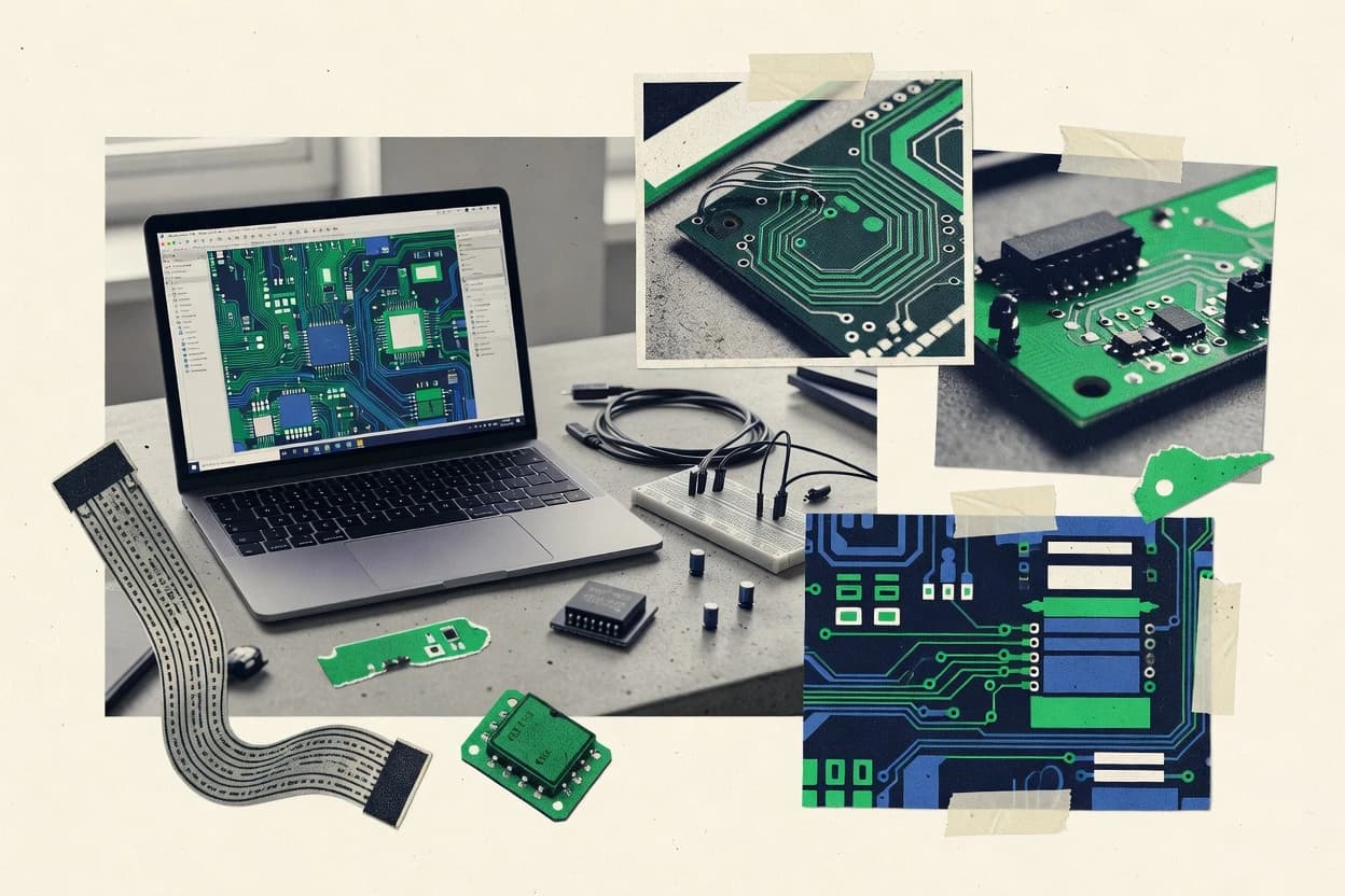
Compare top Electronic Circuit Design Software tools with ranked picks like Altium Designer and Mentor Expedition PCB for faster PCB design decisions.

How we ranked these tools
Core product claims cross-referenced against official documentation, changelogs, and independent technical reviews.
Analyzed video reviews and hundreds of written evaluations to capture real-world user experiences with each tool.
AI persona simulations modeled how different user types would experience each tool across common use cases and workflows.
Final rankings reviewed and approved by our editorial team with authority to override AI-generated scores based on domain expertise.
Score: Features 40% · Ease 30% · Value 30%
Gitnux may earn a commission through links on this page — this does not influence rankings. Editorial policy
Editor’s top 3 picks
Three quick recommendations before you dive into the full comparison below — each one leads on a different dimension.
Altium Designer
Integrated schematic-to-layout design rules with real-time cross probing
Built for professional PCB design teams needing rigorous rules and full workflow automation.
Cadence OrCAD Capture and PCB Designer
Editor pickCapture-to-PCB design rule-driven connectivity validation across the full schematic and layout workflow
Built for teams designing boards with complex schematics and rules-driven PCB layout.
Mentor Expedition PCB
Editor pickConstraint-driven routing and verification to enforce manufacturing-ready design rules
Built for large electronics programs needing rule-driven PCB layout and signoff readiness.
Related reading
Comparison Table
This comparison table evaluates electronic circuit design and PCB layout software, including Altium Designer, Cadence OrCAD Capture with PCB Designer, Mentor Expedition PCB, KiCad, and Autodesk Fusion Electronics. It contrasts core workflow differences such as schematic capture, library management, PCB rules checking, simulation integration, and output formats so teams can match tool capabilities to specific design requirements.
Altium Designer
PCB CADProvides schematic capture, PCB layout, signal integrity, and manufacturing-ready outputs for electronics design and production workflows.
Integrated schematic-to-layout design rules with real-time cross probing
Altium Designer stands out for deep end-to-end PCB design with tight schematic-to-layout integration and advanced routing control. It supports multi-channel design workflows with hierarchical schematics, component parameter management, and constraint-driven rule checking.
The PCB editor includes real-time 3D visualization, extensive placement and routing tools, and comprehensive manufacturing outputs from a single project. Collaboration is strengthened by project versioning and workflow tools that tie libraries, designs, and outputs into one governed workspace.
- +Schematic-to-PCB integration keeps net integrity throughout complex changes
- +Constraint-driven design rules reduce layout mistakes and ERC-to-DRC gaps
- +Real-time 3D PCB view helps validate clearances and component keepouts
- +Advanced routing tools support controlled stackups and differential pairs
- –Performance can drop on very large projects with heavy 3D use
- –Learning curve is steep due to dense rules, libraries, and workflows
- –Library management takes careful setup for consistent parameter handling
- –Some tasks feel tool-heavy compared with simpler PCB editors
Best for: Professional PCB design teams needing rigorous rules and full workflow automation
Cadence OrCAD Capture and PCB Designer
PCB CADDelivers schematic capture and PCB layout with constraint-driven design rule checking and manufacturing data preparation.
Capture-to-PCB design rule-driven connectivity validation across the full schematic and layout workflow
Cadence OrCAD Capture and PCB Designer stands out by pairing schematic capture with PCB layout in a unified, industry-focused workflow. The tool supports hierarchical schematics, net connectivity management, and rules-driven PCB design across footprints and routing.
OrCAD Capture integrates component placement intent with PCB Designer through direct design handoff, reducing manual translation steps. Power-centric editing, connectivity checks, and fabrication-oriented outputs support end-to-end board development.
- +Tight schematic-to-PCB handoff maintains net connectivity with fewer manual steps
- +Rules-based design checks catch DRC-style issues during layout work
- +Hierarchical schematic support helps manage complex multi-sheet designs
- +Fabrication-centric output generation supports assembly and board production workflows
- +Component footprint and routing tools streamline layout iteration
- –Legacy OrCAD flow requires careful setup for consistent design-rule behavior
- –Library and footprint management can be time-consuming for bespoke parts
- –Advanced SI tasks may require external specialization beyond basic workflows
- –Workflow customization options can feel less modern than newer EDA suites
Best for: Teams designing boards with complex schematics and rules-driven PCB layout
Mentor Expedition PCB
PCB CADOffers schematic and PCB design with layout automation and constraint-based editing for manufacturing-focused releases.
Constraint-driven routing and verification to enforce manufacturing-ready design rules
Mentor Expedition PCB stands out for deep, enterprise-grade layout workflows built around constraint-driven design and industrial data management. It supports full PCB layout from schematic-driven placement to routing, with advanced rule checking and signoff-oriented verification.
Strong simulation handoff is supported through integration paths that connect design intent, manufacturing outputs, and verification artifacts. Extensive reuse and standardization features help teams manage libraries, design variants, and revision control across large programs.
- +Constraint-based routing and rule checking improve layout correctness early
- +Robust ECO and revision workflows support controlled design changes
- +Strong design data management supports large teams and complex programs
- –Deep configuration complexity increases setup and training time
- –Workflow flexibility can slow teams without strict design standards
Best for: Large electronics programs needing rule-driven PCB layout and signoff readiness
KiCad
Open-source CADEnables schematic capture, PCB layout, and Gerber-based manufacturing outputs through an open-source electronics design toolchain.
Hierarchical schematic design with automated electrical rule and connectivity verification
KiCad stands out for providing a complete open source electronics workflow that spans schematic capture, PCB layout, and manufacturing outputs in one toolchain. Schematic sheets support hierarchical design and net connectivity checks that help catch wiring and pin inconsistencies early.
The PCB editor includes interactive placement, rule-based design checks, and generation of Gerber, drill, and pick-and-place deliverables for common fabrication pipelines. Component libraries support symbol and footprint management so teams can standardize design blocks across projects.
- +Hierarchical schematics with strong net connectivity checking
- +Rule-based design checks catch clearance and footprint issues
- +Generates Gerber and drill outputs for fabrication workflows
- +Reusable symbol and footprint libraries for consistent design blocks
- –Large projects can feel slower during interactive PCB editing
- –Advanced routing strategies require manual guidance and tuning
- –3D visualization is functional but not as detailed as dedicated viewers
- –Library management needs disciplined structure to avoid footprint drift
Best for: Open source circuit designers needing full schematic-to-PCB deliverables
Autodesk Fusion Electronics
Unified CADSupports electronics schematic and PCB design integrated with a larger CAD ecosystem for model-based engineering workflows.
3D PCB visualization integrated with mechanical design for enclosure fit validation
Autodesk Fusion Electronics stands out with a unified flow that links schematic design to PCB layout and 3D visualization. The workspace supports component placement, routing, and design-rule checks for manufacturable PCB geometries.
It also brings electronics data into the broader Fusion ecosystem for mechanical and electrical coordination through shared models. This helps teams validate enclosure fit and keep electrical and physical design changes synchronized.
- +Tight schematic-to-layout workflow with consistent electrical data across tools
- +3D PCB and assembly visualization helps verify fit with mechanical components
- +Design rule checks catch common routing and clearance issues
- +Library management supports structured component reuse across projects
- –Complex multi-board design organization can feel cumbersome
- –Advanced constraint automation is less extensive than specialized EDA suites
- –Large legacy netlist workflows may require extra cleanup steps
- –Component footprint quality depends heavily on imported library accuracy
Best for: Teams needing synchronized electrical and mechanical design with strong 3D context
DipTrace
PCB CADCombines schematic capture and PCB layout with autoplacement and autorouting features aimed at production-ready board designs.
Hierarchical schematic design with ERC checks and immediate netlist-driven PCB transfer
DipTrace stands out for offering an integrated workflow that goes from schematic capture to PCB layout within one desktop application. Schematic features include hierarchical blocks and electrical rule checking to reduce connectivity mistakes.
PCB design supports autorouting and detailed board editing with constraint-based design rules. Component management includes library tools for symbol and footprint creation and editing.
- +Integrated schematic capture and PCB layout in one desktop workflow
- +Autorouting with design rules helps speed up board routing
- +Electrical rule checking highlights net and connectivity issues
- +Library editor supports custom symbols and footprints
- –Learning curve for advanced layout constraints and routing control
- –High-density designs can feel slower on large projects
- –Component data preparation requires manual symbol and footprint setup often
Best for: Hobbyist to mid-size projects needing tight schematic-to-PCB integration
Target 3001!
PCB CADProvides schematic and PCB layout for producing manufacturing files with component libraries and design rule checks.
Netlist-driven schematic to PCB consistency checks
Target 3001! focuses on schematic capture and printed-circuit-board layout in an integrated Elektor-branded workflow. The editor supports library parts, netlist-driven connectivity checks, and board routing with consistent design rules.
It also includes autorouting and interactive placement tools aimed at producing manufacturable PCB layouts. The tool is designed around hardware design tasks rather than general diagramming, with project management centered on electronics connectivity.
- +Tight schematic-to-PCB workflow using netlist connectivity
- +Interactive placement and routing tools for PCB layout work
- +Design rule checks catch common constraint and connectivity issues
- +Autorouting supports faster initial board routing
- –Library management and part definition can feel rigid
- –Routing outcomes may require frequent manual cleanup
- –Component footprint accuracy demands careful verification
- –Workflow can be heavy for very small single-board projects
Best for: PCB designers needing integrated schematic capture and routing tools
Simulink
Model-based simulationEnables model-based design and simulation for embedded electronics and system-level behavior that informs circuit requirements.
Simscape Electrical for physical modeling of electromechanical and circuit networks
Simulink distinguishes itself with model-based design for dynamic systems using a graphical block environment and simulation solvers. For electronic circuit design workflows, it supports co-simulation with external SPICE tools through standard interfaces and enables controller and power electronics modeling.
It integrates MATLAB scripting for parameter sweeps, automated report generation, and hardware-facing workflows when models must connect to physical interfaces. Large designs benefit from reusable subsystems, signal logging, and model validation tooling geared toward correctness and performance.
- +Graphical block modeling accelerates verification of control and mixed-signal behaviors
- +Tight MATLAB integration enables scripted parameter sweeps and automated analyses
- +Signal logging and test harnesses support repeatable simulation-based validation
- –Native circuit component modeling is limited compared to dedicated SPICE engines
- –High-fidelity analog behavior often requires external SPICE co-simulation
- –Large models can become complex to manage without strict architecture discipline
Best for: Teams validating mixed-signal control logic with simulation and co-simulation workflows
EPLAN Electric P8
Electrical engineeringSupports electrical schematic engineering with data structures for bills of materials and manufacturing documentation.
Integrated cable and wiring route planning synchronized with schematic and terminal information
EPLAN Electric P8 stands out with tight engineering integration between schematic design and electrical documentation workflows. The software provides route planning for cable and wiring paths plus data-driven generation of bills of materials and terminal layouts.
It supports reusable libraries for components and symbols and uses structured tagging to keep documents consistent. Strong cross-referencing and error checking help teams trace dependencies across projects as designs evolve.
- +Route planning connects wire paths to schematic and terminal data
- +Automated bills of materials and terminal allocation reduce manual reconciliation
- +Cross-references and consistency checks detect symbol, tag, and connection issues early
- –Workflow depends on structured master data setup for consistent tagging
- –Complex projects can feel heavy without disciplined layout and naming conventions
- –Legacy library customization requires careful management across engineering standards
Best for: Manufacturing and engineering teams producing large electrical documentation sets
How to Choose the Right Electronic Circuit Design Software
This buyer's guide explains how to choose Electronic Circuit Design Software for schematic capture, PCB layout, and manufacturing deliverables. It covers Altium Designer, Cadence OrCAD Capture and PCB Designer, Mentor Expedition PCB, KiCad, Autodesk Fusion Electronics, DipTrace, Target 3001!, Simulink, EPLAN Electric P8, and the workflows they represent. The guide focuses on concrete capabilities like constraint-driven rules, schematic-to-layout connectivity, and 3D visualization.
What Is Electronic Circuit Design Software?
Electronic Circuit Design Software is a toolchain that turns electrical intent into schematics, checks connectivity and rules, and produces PCB or documentation outputs. It solves wiring and footprint consistency issues by running ERC-style checks and DRC-style constraint rules during design. It also supports fabrication-ready exports like Gerber and drill files for PCB workflows. Tools like Altium Designer and KiCad show what a full schematic-to-PCB workflow looks like in practice.
Key Features to Look For
The strongest tools reduce costly design breaks by enforcing connectivity and manufacturability through rules, handoffs, and exports.
Integrated schematic-to-layout connectivity with real-time cross probing
Altium Designer enforces schematic-to-layout design rules with real-time cross probing so net integrity survives complex changes. This same goal appears as capture-to-PCB design rule-driven connectivity validation in Cadence OrCAD Capture and PCB Designer.
Constraint-driven routing and verification for manufacturing-ready rules
Mentor Expedition PCB uses constraint-driven routing and verification to enforce manufacturing-ready design rules early. KiCad adds rule-based design checks that catch clearance and footprint issues during PCB editing.
Automated electrical rule checking with hierarchical schematics
KiCad provides hierarchical schematic design with automated electrical rule and connectivity verification. DipTrace and Target 3001! also support hierarchical schematic workflows with ERC checks that highlight net and connectivity issues.
Fabrication and documentation deliverables from a single governed workflow
Altium Designer generates comprehensive manufacturing outputs from one project tied into a governed workspace. Cadence OrCAD Capture and PCB Designer is fabrication-centric and prepares manufacturing data as part of the schematic-to-layout flow.
Real-time 3D PCB visualization and mechanical fit context
Altium Designer includes real-time 3D PCB visualization to validate clearances and component keepouts. Autodesk Fusion Electronics integrates 3D PCB and assembly visualization to verify enclosure fit with mechanical design coordination.
Simulation-first system validation and physical network modeling
Simulink supports graphical block modeling for dynamic systems and uses tight MATLAB integration for scripted parameter sweeps and automated analyses. Simscape Electrical provides physical modeling of electromechanical and circuit networks, and it connects to external SPICE via co-simulation paths for high-fidelity analog behavior.
How to Choose the Right Electronic Circuit Design Software
A practical selection path maps the design workflow needs first, then matches rule enforcement, handoffs, and deliverables to the project reality.
Start with the end deliverable to match the tool’s core workflow
For PCB production deliverables, choose a tool centered on schematic-to-PCB design and export generation like Altium Designer, KiCad, Cadence OrCAD Capture and PCB Designer, or Mentor Expedition PCB. For enclosure fit and synchronized electrical and mechanical design, Autodesk Fusion Electronics matches the need because its workflow ties 3D PCB visualization directly to mechanical context.
Pick the level of schematic-to-PCB rule enforcement that matches project risk
High-risk designs with frequent schematic changes benefit from Altium Designer because integrated schematic-to-layout design rules and real-time cross probing reduce net integrity breaks. Teams also needing strong capture-to-PCB validation can use Cadence OrCAD Capture and PCB Designer for capture-to-PCB design rule-driven connectivity validation.
Match routing and design checks to manufacturing readiness expectations
If manufacturing-ready signoff and controlled ECO processes are required, Mentor Expedition PCB offers constraint-driven routing and verification plus robust ECO and revision workflows. If the priority is open-source full deliverables with rule-based clearance and footprint checks, KiCad provides hierarchical design with automated electrical rule and connectivity verification plus Gerber and drill output generation.
Choose the tool whose library and data workflow will not break under real part complexity
Altium Designer supports component parameter management but requires careful library management setup for consistent parameter handling. OrCAD and PCB Designer also place emphasis on library and footprint management for bespoke parts, while Target 3001! and DipTrace rely on careful component footprint accuracy verification when part data needs preparation.
Use simulation and system modeling tools only when system behavior validation is the bottleneck
When the project bottleneck is control logic, mixed-signal system behavior, or repeated parameter sweeps, Simulink accelerates validation through graphical block modeling and MATLAB-driven workflows. When physical network modeling of electromechanical and circuit networks drives correctness, Simscape Electrical in Simulink provides that modeling path and can use co-simulation for SPICE-backed analog fidelity.
Who Needs Electronic Circuit Design Software?
Different Electronic Circuit Design Software tools target different engineering workflows from high-volume PCB rule enforcement to system modeling and large documentation sets.
Professional PCB design teams that need rigorous rules and full end-to-end workflow automation
Altium Designer fits professional teams because integrated schematic-to-layout design rules with real-time cross probing keep net integrity stable during complex changes. Mentor Expedition PCB also matches large programs that require constraint-driven routing and verification for signoff readiness.
Teams designing boards with complex schematics and rules-driven layout
Cadence OrCAD Capture and PCB Designer targets complex multi-sheet schematics through hierarchical schematic support and capture-to-PCB design rule-driven connectivity validation. This combination reduces manual translation steps during handoff between schematic intent and layout execution.
Large electronics programs that prioritize revision control and signoff-oriented verification
Mentor Expedition PCB is built for enterprise workflows with robust ECO and revision workflows plus constraint-driven routing and verification. Teams that need strict design standards benefit from the system’s early enforcement of manufacturing-ready rules.
Open-source circuit designers that need a complete schematic-to-PCB deliverable toolchain
KiCad supports hierarchical schematics with automated electrical rule and connectivity verification and outputs Gerber, drill, and pick-and-place deliverables. This makes it a strong fit for open-source workflows that must still produce fabrication-ready files.
Common Mistakes to Avoid
Misalignment between the tool’s workflow and the project’s deliverables leads to avoidable rework in connectivity, routing, and verification.
Expecting schematic edits to automatically preserve net integrity without real cross probing
Tools like Altium Designer and Cadence OrCAD Capture and PCB Designer are built around schematic-to-PCB design rule-driven connectivity validation with real-time cross probing or capture-to-PCB handoff validation. Tools that rely more on manual cleanup can increase the chance that connectivity intent drifts during layout.
Relying on advanced routing without matching constraint complexity to team capability
Mentor Expedition PCB uses constraint-driven routing and verification that improves correctness early but increases setup and training time. Altium Designer also has a steep learning curve due to dense rules and workflows, so teams should plan training time rather than only migrating project files.
Underestimating library and footprint accuracy as a source of layout and fabrication issues
KiCad requires disciplined symbol and footprint library structure to prevent footprint drift, and DipTrace and Target 3001! often depend on manual symbol and footprint setup and verification. Altium Designer and OrCAD also require careful library management for consistent parameter handling and stable footprint behavior.
Choosing a simulation-first tool for PCB signoff without SPICE-accurate component behavior
Simulink supports dynamic system validation with MATLAB integration, but its native circuit component modeling is limited compared with dedicated SPICE engines. Simscape Electrical in Simulink helps with physical modeling and can use co-simulation paths to external SPICE tools when high-fidelity analog behavior is required.
How We Selected and Ranked These Tools
we evaluated each tool on three sub-dimensions. Features carried a weight of 0.4. Ease of use carried a weight of 0.3. Value carried a weight of 0.3. The overall rating is computed as overall = 0.40 × features + 0.30 × ease of use + 0.30 × value. Altium Designer separated itself from lower-ranked tools through integrated schematic-to-layout design rules with real-time cross probing, which directly boosted the features sub-dimension by reducing connectivity and rule-check mismatches across complex PCB changes.
Frequently Asked Questions About Electronic Circuit Design Software
Which tool best supports a full schematic-to-PCB workflow with tight integration and rule enforcement?
What software is most suitable for hierarchical schematics and connectivity verification early in the design process?
Which platform is optimized for enterprise-grade PCB layout, signoff readiness, and industrial data management?
Which electronic design tool is best for designers who need strong 3D visualization and mechanical fit validation?
Which option is most appropriate for a desktop workflow that stays focused on schematic capture and PCB layout without switching tools?
Which software is strongest for mixed-signal and control system verification using model-based design?
Which tool is best for large electrical documentation work that includes BOM generation and terminal data consistency?
Which option best supports cable and wiring route planning tied to schematic and terminal information?
Which software helps prevent routing and connectivity mistakes by enforcing design rules throughout capture-to-layout handoff?
What starting workflow is fastest for teams that want immediate fabrication outputs without complex toolchain setup?
Conclusion
After evaluating 9 manufacturing engineering, Altium Designer stands out as our overall top pick — it scored highest across our combined criteria of features, ease of use, and value, which is why it sits at #1 in the rankings above.
Use the comparison table and detailed reviews above to validate the fit against your own requirements before committing to a tool.
Tools reviewed
Primary sources checked during evaluation.
Referenced in the comparison table and product reviews above.
Keep exploring
Comparing two specific tools?
Software Alternatives
See head-to-head software comparisons with feature breakdowns, pricing, and our recommendation for each use case.
Explore software alternatives→In this category
Manufacturing Engineering alternatives
See side-by-side comparisons of manufacturing engineering tools and pick the right one for your stack.
Compare manufacturing engineering tools→FOR SOFTWARE VENDORS
Not on this list? Let’s fix that.
Our best-of pages are how many teams discover and compare tools in this space. If you think your product belongs in this lineup, we’d like to hear from you—we’ll walk you through fit and what an editorial entry looks like.
Apply for a ListingWHAT THIS INCLUDES
Where buyers compare
Readers come to these pages to shortlist software—your product shows up in that moment, not in a random sidebar.
Editorial write-up
We describe your product in our own words and check the facts before anything goes live.
On-page brand presence
You appear in the roundup the same way as other tools we cover: name, positioning, and a clear next step for readers who want to learn more.
Kept up to date
We refresh lists on a regular rhythm so the category page stays useful as products and pricing change.