GITNUXSOFTWARE ADVICE
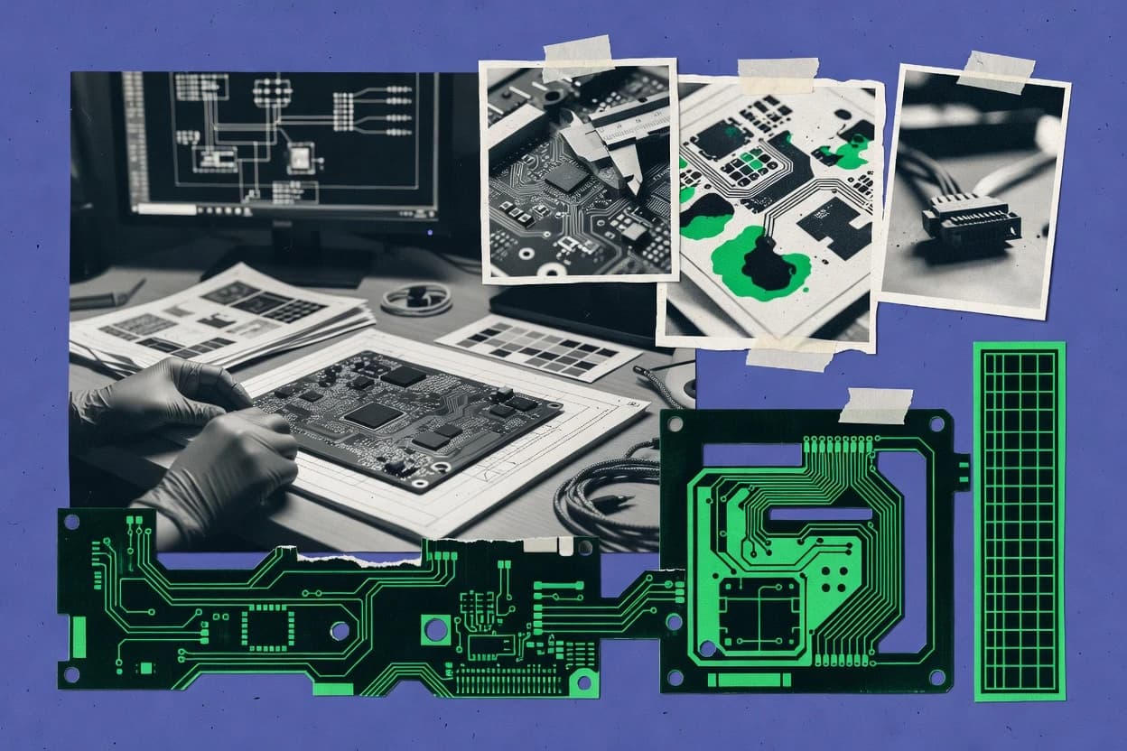
Manufacturing EngineeringTop 10 Best Electronic Design Automation Software of 2026
Top 10 Electronic Design Automation Software picks with a ranking and comparison for PCB and schematic design, including Cadence Allegro and Altium.

How we ranked these tools
Core product claims cross-referenced against official documentation, changelogs, and independent technical reviews.
Analyzed video reviews and hundreds of written evaluations to capture real-world user experiences with each tool.
AI persona simulations modeled how different user types would experience each tool across common use cases and workflows.
Final rankings reviewed and approved by our editorial team with authority to override AI-generated scores based on domain expertise.
Score: Features 40% · Ease 30% · Value 30%
Gitnux may earn a commission through links on this page — this does not influence rankings. Editorial policy
Editor’s top 3 picks
Three quick recommendations before you dive into the full comparison below — each one leads on a different dimension.
Cadence Allegro PCB Designer
Constraint manager plus impedance and length tuning during interactive routing
Built for teams building high-speed PCBs needing constraint enforcement at scale.
Altium Designer
Editor pickConstraint-driven design rules with real-time PCB routing feedback
Built for teams building complex PCBs needing rule-based design, reuse, and verification.
KiCad
Editor pickPCB design rule checks with interactive routing feedback in the same editor
Built for engineers and makers needing a full EDA toolchain without vendor lock-in.
Related reading
Comparison Table
This comparison table evaluates Electronic Design Automation tools used across schematic capture, PCB layout, simulation, and embedded control workflows. It contrasts Cadence Allegro PCB Designer, Altium Designer, KiCad, dSPACE, MathWorks Simulink, and other common options by capability and typical fit for different engineering teams. Readers can use the side-by-side entries to map design and verification requirements to the most relevant software category.
Cadence Allegro PCB Designer
PCB designAllegro enables high-performance PCB design with constraint-driven layout, verification, and fabrication data generation for complex electronics.
Constraint manager plus impedance and length tuning during interactive routing
Cadence Allegro PCB Designer stands out for its integration of high-speed layout, constraint-driven design, and advanced signal integrity flows in one PCB engineering environment. Core capabilities include schematic-to-PCB connectivity, constraint management, interactive routing with length and impedance targets, and robust DRC checks.
It also supports large, complex designs with hierarchical reuse, effective plane and copper management, and manufacturing-ready output generation. For teams that handle tight performance requirements, the workflow emphasizes rule enforcement and predictable routing behavior across net classes.
- +Constraint-driven routing supports length and impedance targets
- +High-speed signal integrity oriented layout checks and workflows
- +Strong DRC coverage for connectivity, spacing, and stackup rules
- +Efficient handling of large, complex PCB projects
- –Setup of advanced constraints can require specialized expertise
- –Workflow tuning can take time for new design teams
- –Interactive routing performance depends heavily on database configuration
- –Licensing and environment management add operational overhead
Best for: Teams building high-speed PCBs needing constraint enforcement at scale
More related reading
Altium Designer
Integrated PCBAltium Designer supports schematic-to-PCB design with constraint-based layout, simulation-ready workflows, and manufacturing document exports.
Constraint-driven design rules with real-time PCB routing feedback
Altium Designer stands out with a unified schematic-to-PCB workflow built around an integrated project environment and tight database control. It supports advanced schematic capture, constraint-driven PCB design, and interactive routing with detailed rules for clearances, stackups, and fabrication constraints.
Design reuse is strong through hierarchical libraries, managed components, and versioned project data for coordinated team work. Verification covers electrical rules checks, integrated 3D PCB visualization, and export-ready outputs for downstream fabrication and assembly workflows.
- +Constraint-driven PCB design with robust clearance and rule checking
- +Interactive routing tools optimized for high-density PCB layouts
- +Integrated 3D visualization tied to the same component geometry
- +Hierarchical schematics with reusable blocks and library management
- +Comprehensive electrical rules checks across schematics and PCB
- –Large project files can slow editing on lower-end workstations
- –Steep learning curve for rule setup and advanced layout features
- –Library maintenance takes discipline to keep components consistent
Best for: Teams building complex PCBs needing rule-based design, reuse, and verification
KiCad
open-source PCBOpen-source schematic capture and PCB layout with project-based libraries, ERC and DRC checks, and outputs for fabrication workflows.
PCB design rule checks with interactive routing feedback in the same editor
KiCad stands out for its complete open-source electronics workflow spanning schematic capture, PCB layout, and verification tools in one package. It supports hierarchical schematics, multi-sheet design, and net connectivity rules that flow directly into PCB routing.
The PCB editor includes interactive routing, footprint management, and design-rule checks that help catch clearances, widths, and assembly constraints before export. Output options cover fabrication and assembly artifacts such as Gerbers, drill files, and 3D viewer assets for model-based inspection.
- +Open workflow from schematic to PCB without tool handoffs
- +Hierarchical multi-sheet schematics with strong netlist consistency
- +Design-rule checks catch clearance, track width, and rule violations early
- +Footprint library management supports parametric linking to symbols
- +Outputs Gerbers, drill data, and pick-and-place friendly exports
- –Advanced constraint workflows can feel manual for large designs
- –3D preview is useful but less integrated than some commercial viewers
- –Library footprint quality varies and requires active curation
- –Large projects can slow down during editing and rule checking
- –Simulation workflows depend on external tools and setup
Best for: Engineers and makers needing a full EDA toolchain without vendor lock-in
dSPACE
HIL simulationModel-based design and real-time hardware-in-the-loop toolchain for validating electronic control behavior using automated deployment workflows.
Hardware-in-the-loop testing using dSPACE real-time target systems and integrated tooling
dSPACE stands out for integrating model-based design with real-time target hardware for automated controller development. It supports rapid prototyping and closed-loop testing using dedicated real-time simulation and hardware-in-the-loop workflows.
Toolchains cover plant modeling, controller implementation, and system validation with measurement, calibration, and logging capabilities. Strong emphasis is placed on scalable automation from early simulation to verification on dSPACE targets.
- +Tight hardware-in-the-loop integration with dSPACE real-time platforms
- +Model-based design workflow supports rapid control development
- +Measurement, calibration, and logging workflows streamline validation
- +End-to-end toolchain supports automation from design to testing
- –Hardware and workflow are tightly coupled to dSPACE environments
- –Setup complexity increases for teams without real-time testing experience
- –Licensing and project configuration can be heavy for small projects
Best for: Teams building controllers with real-time HIL validation on dSPACE targets
MathWorks Simulink
model-based designModel-based design environment for generating electronics control models and automated test workflows that integrate with hardware targets.
Hardware-in-the-loop simulation via Simulink for real-time plant and controller verification
Simulink stands out for modeling, simulating, and verifying embedded control and signal-processing systems using a block-diagram workflow. It supports system-level architecture with toolboxes for code generation, model reference, and hardware-in-the-loop test connectivity.
It integrates with MATLAB for scripting, data handling, and algorithm development, which enables repeatable analysis and regression testing. For electronic design automation work, it connects behavioral models to implementation targets through model-to-code and test automation pipelines.
- +Block-diagram modeling for complex embedded control and signal-processing systems
- +Automatic code generation from models to accelerate implementation
- +Hardware-in-the-loop workflows for validating real-time behavior
- +Model reference supports scalable team development and modular reuse
- +Extensive simulation and analysis tooling for verification
- –Modeling discipline required to keep large diagrams maintainable
- –Graphics-heavy workflows can slow fast iteration for some teams
- –System integration effort needed for multi-tool EDA toolchains
Best for: Teams building embedded controllers and validating behavior before hardware release
Logisim-evolution
logic simulationAn open-source digital logic simulator that supports logic design validation for manufacturing test development.
Interactive waveform and signal tracing tightly integrated with schematic simulation
Logisim-evolution stands out for interactive, schematic-level logic design with immediate visual feedback. It supports building and simulating combinational and sequential circuits using built-in gates, integrated components, and custom wiring.
The tool includes timing-oriented simulation elements and lets projects grow with user-defined components and reusable subcircuits. It is best suited to teaching, prototyping, and validating small digital systems rather than large-scale physical implementation.
- +Instant visual simulation with clear signal propagation
- +Rich library of digital gates and sequential components
- +User-defined components enable reusable subcircuits
- +Works well for education, debugging, and rapid prototyping
- –Limited or absent support for ASIC or FPGA physical design steps
- –Scalability becomes difficult for very large circuit schematics
- –Hardware-verified flows like synthesis and place-and-route are not covered
- –Timing analysis remains schematic-focused rather than production-grade
Best for: Teaching and prototyping small digital circuits with visual simulation
FreeCAD EDA Workbench
CAD-assisted EDAA community-driven EDA capability inside FreeCAD for preliminary electrical modeling and exported documentation workflows.
Single FreeCAD document workflow linking schematics and PCB geometry for co-design
FreeCAD EDA Workbench distinguishes itself by bringing schematic and PCB-centric workflows into the FreeCAD modeling environment. The workbench supports creating and editing circuit schematics, then generating and managing PCB elements aligned to FreeCAD’s geometry and project structure.
It is strongest for teams that want EDA objects and mechanical models to share the same underlying CAD workspace. Board design tasks focus on component placement, footprint handling, and routing workflows designed to interoperate with FreeCAD projects.
- +Integrates EDA work with FreeCAD geometry for electronics-mechanical co-design
- +Schematic drafting and board data stay in the same workspace ecosystem
- +Footprint-oriented board creation leverages FreeCAD modeling tools
- +Project structure aligns with FreeCAD document organization
- –Routing and advanced signal constraints are limited versus dedicated PCB tools
- –Large design performance and scalability can lag established EDA suites
- –Library maturity for components and footprints varies by community content
- –Export to vendor-ready manufacturing outputs may require extra steps
Best for: Teams needing PCB and mechanical CAD integration inside FreeCAD workflows
EasyEDA
cloud PCB designA browser-based schematic capture and PCB layout platform that exports manufacturing files for production.
Integrated browser editor that supports schematic capture and PCB layout in one project workspace
EasyEDA stands out with a browser-first workflow that keeps schematic capture and PCB layout accessible from any device. It combines schematic symbols and PCB footprint libraries with automatic ERC and DRC checks to reduce common design errors.
The editor supports net connectivity rules, layer stacks, and polygon pours for practical board routing and fabrication readiness. Collaboration is enabled through shareable design links and versioned project files stored in the EasyEDA environment.
- +Browser-based schematic and PCB layout avoids desktop tool installation friction
- +Built-in symbol and footprint library speeds up component selection
- +ERC and DRC catch connectivity and rule violations before export
- –Complex constraints and advanced routing controls can feel limited
- –Footprint accuracy still depends on manual review of imported parts
- –Large multi-sheet projects can feel slower during editing
Best for: Teams and individuals designing PCBs with fast web-based capture and layout
Upverter
web-based PCBAn online schematic and PCB design tool that produces manufacturing outputs for electronics projects.
Cloud project collaboration with shared schematic and PCB artifacts.
Upverter stands out for a browser-based EDA workflow that keeps schematic and PCB work accessible without local tool setup. It provides schematic capture and PCB layout with a managed component library workflow and rules-driven design validation.
The platform supports collaborative design review and project sharing around hardware artifacts. It also includes simulation-oriented and export-focused flows for common electronic design handoffs.
- +Browser-based schematic and PCB editing reduces local tool friction.
- +Integrated design-rule checks catch constraint issues during layout.
- +Collaborative projects enable review and sharing of design artifacts.
- –Advanced workflows may feel constrained compared to desktop-centric EDA suites.
- –Simulation capabilities are not as deep as dedicated simulator-first toolchains.
- –Complex custom footprints and libraries require careful management.
Best for: Teams needing cloud-based schematic and PCB workflows with collaboration.
Proteus Design Suite
mixed-mode simulationA mixed-mode schematic capture and simulation suite with virtual instrumentation for validating electronics behavior.
Instrument-based simulation that drives and measures designs through virtual test equipment
Proteus Design Suite blends schematic capture, simulation, and PCB layout into a single workflow for electronics projects. It supports mixed-signal simulation with instrument-level test setups, so designs can be validated beyond digital-only behavior. The library management and component symbol linkage streamline building testable schematics that connect directly into simulation runs and board creation.
- +Mixed-signal simulation supports real instrument testbench setups
- +Integrated schematic-to-layout workflow reduces handoff errors
- +Large component models library accelerates new circuit assembly
- +Event-driven simulation helps validate timing and control logic
- –Advanced verification depends on availability of accurate device models
- –Complex multi-rail test setups can become labor-intensive to maintain
- –Large projects may slow down during full simulation and export
Best for: Teams validating analog, digital, and mixed-signal designs in one workflow
How to Choose the Right Electronic Design Automation Software
This buyer’s guide helps teams choose Electronic Design Automation Software by matching tool capabilities to real design workflows. It covers PCB-centric suites like Cadence Allegro PCB Designer and Altium Designer, open and browser options like KiCad and EasyEDA, and simulation and model-based toolchains like MathWorks Simulink and Proteus Design Suite. It also explains when control validation tools like dSPACE fit better than traditional PCB editors.
What Is Electronic Design Automation Software?
Electronic Design Automation Software is a set of tools that turn schematic intent into validated electronics designs using simulation, rule checks, and manufacturing output generation. For PCB work, tools like Cadence Allegro PCB Designer and Altium Designer manage schematic-to-PCB connectivity, enforce clearances and stackup constraints, and generate fabrication-ready outputs. For embedded and control electronics, MathWorks Simulink and dSPACE support model-based design and hardware-in-the-loop validation to verify real-time behavior before hardware release.
Key Features to Look For
The strongest EDA choices make design intent enforceable with the right kind of verification at the right stage.
Constraint-driven PCB routing with length and impedance targeting
Cadence Allegro PCB Designer uses a constraint manager that supports impedance and length tuning during interactive routing. Altium Designer delivers constraint-driven design rules with real-time PCB routing feedback for clearances, stackups, and fabrication constraints.
Integrated design rule checks tied to routing feedback
KiCad provides PCB design rule checks with interactive routing feedback in the same editor. EasyEDA also includes automatic ERC and DRC checks that catch connectivity and rule violations before export.
Schematic-to-PCB connectivity with hierarchical reuse and managed libraries
Altium Designer supports hierarchical schematics with reusable blocks and library management that keeps complex projects coordinated. Cadence Allegro PCB Designer supports schematic-to-PCB connectivity and hierarchical reuse for large designs.
Manufacturing-ready output generation and fabricator-friendly exports
Cadence Allegro PCB Designer focuses on manufacturing-ready output generation supported by strong DRC coverage for connectivity, spacing, and stackup rules. KiCad outputs Gerbers and drill files plus 3D viewer assets for fabrication and inspection workflows.
Model-based design and hardware-in-the-loop validation
dSPACE provides model-based design plus tight hardware-in-the-loop integration using dSPACE real-time target systems. MathWorks Simulink supports hardware-in-the-loop workflows that validate real-time plant and controller behavior before hardware release.
Mixed-signal and instrument-based simulation inside the design workflow
Proteus Design Suite combines schematic capture with mixed-signal simulation using instrument-level test setups. Logisim-evolution provides interactive waveform and signal tracing tightly integrated with schematic simulation for small digital circuit validation.
How to Choose the Right Electronic Design Automation Software
Selection should start from the verification target, then confirm the tool can enforce constraints and produce outputs without risky handoffs.
Start with the end validation you must complete
If the deliverable requires constraint enforcement for high-speed PCB performance, Cadence Allegro PCB Designer fits because it supports impedance and length tuning during interactive routing. If the deliverable requires rule-based PCB design with immediate routing feedback, Altium Designer fits because its constraint-driven design rules provide real-time routing feedback.
Match schematic-to-PCB workflow depth to project complexity
For large boards that rely on hierarchical reuse and strong connectivity integrity, Cadence Allegro PCB Designer supports schematic-to-PCB connectivity plus hierarchical reuse. For complex PCB work that also needs hierarchical blocks and reusable libraries, Altium Designer supports hierarchical schematics with reusable blocks and managed components.
Confirm the rule checks that prevent the specific failures seen in layout
If the biggest risk is clearance, spacing, and stackup violations, Cadence Allegro PCB Designer is built around strong DRC coverage for connectivity, spacing, and stackup rules. If the biggest risk is catching rule violations early while iterating interactively, KiCad and EasyEDA both provide DRC and interactive error detection tied to the layout workflow.
Choose the simulation tool that matches the real test environment
If validation must happen on real hardware targets, dSPACE is designed for hardware-in-the-loop testing using dSPACE real-time target systems. If the validation needs to occur through model-based workflows and code generation, MathWorks Simulink supports hardware-in-the-loop simulation via Simulink for real-time plant and controller verification.
Pick the collaboration and workflow model that teams can actually run
If cloud collaboration is the priority, Upverter supports browser-based schematic and PCB editing with cloud project collaboration and shared schematic and PCB artifacts. If mechanical co-design is required in the same CAD workspace, FreeCAD EDA Workbench supports linking schematics and PCB geometry inside FreeCAD.
Who Needs Electronic Design Automation Software?
Different EDA tools serve different portions of the electronics lifecycle from PCB layout to system-level validation and hardware-in-the-loop testing.
High-speed PCB teams that must enforce impedance and length across large designs
Cadence Allegro PCB Designer fits teams building high-speed PCBs that need constraint enforcement at scale because its constraint manager supports impedance and length tuning during interactive routing. It also supports efficient handling of large, complex PCB projects and strong DRC coverage for connectivity, spacing, and stackup rules.
PCB teams building complex boards that need rule-based design, reuse, and verification
Altium Designer fits teams building complex PCBs that need rule-based design, reuse, and verification because it provides constraint-driven design rules and real-time PCB routing feedback. It also supports integrated 3D PCB visualization tied to component geometry and comprehensive electrical rules checks across schematics and PCB.
Engineers and makers who want an end-to-end open electronics workflow
KiCad fits engineers and makers needing a full EDA toolchain without vendor lock-in because it provides open-source schematic capture, PCB layout, and verification checks in one package. It also exports Gerbers, drill files, and 3D viewer assets suitable for fabrication workflows.
Control development teams that need real-time hardware-in-the-loop validation
dSPACE fits teams building controllers with real-time HIL validation on dSPACE targets because it integrates model-based design with real-time hardware-in-the-loop testing and includes measurement, calibration, and logging workflows. MathWorks Simulink fits teams validating embedded control behavior before hardware release using hardware-in-the-loop simulation connected to real-time targets.
Common Mistakes to Avoid
The most costly failures come from picking a tool that cannot enforce the right constraints, cannot produce the right verification artifacts, or cannot fit the required workflow model.
Treating constraint setup as a one-time task instead of a workflow capability
Cadence Allegro PCB Designer can require specialized expertise to set up advanced constraints and tune interactive routing behavior, so planning training and database configuration time avoids late surprises. Altium Designer also has a steep learning curve for rule setup and advanced layout features, so teams should allocate time to establish clear design rules early.
Assuming web or open tools automatically match desktop constraint depth for high-density boards
EasyEDA and Upverter both provide integrated DRC and constraint-based validation, but complex constraints and advanced routing controls can feel limited compared with desktop-centric suites. KiCad supports rule checks and interactive routing feedback, but advanced constraint workflows can feel manual for large designs.
Using PCB-only workflows for real-time behavior validation
dSPACE and MathWorks Simulink are built for hardware-in-the-loop and real-time plant and controller verification, so using a pure PCB tool for controller timing confirmation leads to missing system-level validation. Proteus Design Suite can validate mixed-signal designs with instrument-based simulation, but it does not replace dSPACE real-time target validation for control hardware.
Relying on inaccurate device models for advanced verification
Proteus Design Suite depends on accurate device models for advanced verification, and complex multi-rail instrument test setups can become labor-intensive. Teams validating analog, digital, and mixed-signal systems should confirm that device libraries and instrument testbenches are maintained consistently in the chosen workflow.
How We Selected and Ranked These Tools
we evaluated every tool on three sub-dimensions: features with weight 0.4, ease of use with weight 0.3, and value with weight 0.3. The overall rating equals 0.40 × features plus 0.30 × ease of use plus 0.30 × value. Cadence Allegro PCB Designer separated itself from lower-ranked tools through concrete feature coverage for high-speed constraint enforcement, including a constraint manager that supports impedance and length tuning during interactive routing. That same capability also paired with strong DRC coverage for connectivity, spacing, and stackup rules, which directly supports predictable routing behavior for complex PCB projects.
Frequently Asked Questions About Electronic Design Automation Software
Which EDA tools provide tight schematic-to-PCB connectivity and rule enforcement in the same workflow?
What tool best supports high-speed PCB routing targets like length and impedance constraints?
Which EDA platform is best suited for teams that need reusable design data and versioned collaboration?
Which tools are strongest for mixed-signal and analog verification alongside digital design?
What EDA workflow fits best when hardware-in-the-loop validation is a requirement?
Which option provides a complete open-source electronics workflow from schematic capture to fabrication outputs?
Which tools emphasize browser-based or cloud-based access for schematic and PCB work?
Which platform is best for co-design when mechanical CAD geometry must stay in sync with PCB objects?
What is the best fit for teaching or prototyping small digital circuits with immediate visual feedback?
Which tools help catch PCB manufacturability issues through integrated verification like DRC and DFM-style checks?
Conclusion
After evaluating 10 manufacturing engineering, Cadence Allegro PCB Designer stands out as our overall top pick — it scored highest across our combined criteria of features, ease of use, and value, which is why it sits at #1 in the rankings above.
Use the comparison table and detailed reviews above to validate the fit against your own requirements before committing to a tool.
Tools reviewed
Primary sources checked during evaluation.
Referenced in the comparison table and product reviews above.
Keep exploring
Comparing two specific tools?
Software Alternatives
See head-to-head software comparisons with feature breakdowns, pricing, and our recommendation for each use case.
Explore software alternatives→In this category
Manufacturing Engineering alternatives
See side-by-side comparisons of manufacturing engineering tools and pick the right one for your stack.
Compare manufacturing engineering tools→FOR SOFTWARE VENDORS
Not on this list? Let’s fix that.
Our best-of pages are how many teams discover and compare tools in this space. If you think your product belongs in this lineup, we’d like to hear from you—we’ll walk you through fit and what an editorial entry looks like.
Apply for a ListingWHAT THIS INCLUDES
Where buyers compare
Readers come to these pages to shortlist software—your product shows up in that moment, not in a random sidebar.
Editorial write-up
We describe your product in our own words and check the facts before anything goes live.
On-page brand presence
You appear in the roundup the same way as other tools we cover: name, positioning, and a clear next step for readers who want to learn more.
Kept up to date
We refresh lists on a regular rhythm so the category page stays useful as products and pricing change.