GITNUXSOFTWARE ADVICE
Manufacturing EngineeringTop 10 Best Schematic Pcb Software of 2026
Explore the best schematic PCB software tools to streamline your design process. Compare features and find the top pick for your needs today.

How we ranked these tools
Core product claims cross-referenced against official documentation, changelogs, and independent technical reviews.
Analyzed video reviews and hundreds of written evaluations to capture real-world user experiences with each tool.
AI persona simulations modeled how different user types would experience each tool across common use cases and workflows.
Final rankings reviewed and approved by our editorial team with authority to override AI-generated scores based on domain expertise.
Score: Features 40% · Ease 30% · Value 30%
Gitnux may earn a commission through links on this page — this does not influence rankings. Editorial policy
Editor’s top 3 picks
Three quick recommendations before you dive into the full comparison below — each one leads on a different dimension.
Altium Designer
Unified schematic-driven PCB design rules with real-time constraint checking
Built for electronics teams building high-complexity schematic-to-PCB designs with rigorous rule checking.
Cadence OrCAD PCB Designer
Editor pickOrCAD Capture to PCB Designer net connectivity linkage for schematic-to-layout consistency
Built for teams using OrCAD Capture who need rule-driven PCB layout and release documentation.
KiCad
Editor pickERC and DRC rule checking with schematic-to-layout net association
Built for hardware teams needing full schematic-to-PCB design with strong rule checking.
Related reading
Comparison Table
This comparison table reviews leading schematic and PCB design tools, including Altium Designer, Cadence OrCAD PCB Designer, KiCad, Autodesk EAGLE, and EasyEDA. It highlights the differences that affect real workflows such as schematic capture, PCB layout capabilities, library management, simulation and collaboration features, and typical integration paths. Readers can use the side-by-side specs to narrow down the best fit for board complexity, budget, and toolchain requirements.
Altium Designer
premium ECADProvides schematic capture and PCB layout with tight ECAD-EDA integration, advanced design rule checking, and manufacturing data outputs for PCB fabrication and assembly.
Unified schematic-driven PCB design rules with real-time constraint checking
Altium Designer stands out for a deeply integrated schematic-to-PCB workflow with shared design intelligence and constraint propagation. It supports advanced PCB layout features like rigid-flex design, interactive routing, and robust library management tied to schematic sheets. The platform also provides schematic-driven design rules, net connectivity checking, and simulation hooks that reduce iteration time from capture to verification.
- +Tight schematic-to-PCB integration keeps nets and rules synchronized end to end.
- +Powerful rigid-flex and differential routing tools support complex stackups.
- +Strong constraint and design rule checking catches connectivity and rule violations early.
- –Complex projects require more configuration to keep libraries and rules consistent.
- –Learning curve is steep for teams used to simpler capture and layout flows.
- –Large designs can feel heavy without careful workspace and constraint setup.
Best for: Electronics teams building high-complexity schematic-to-PCB designs with rigorous rule checking
More related reading
Cadence OrCAD PCB Designer
pro ECADDelivers schematic capture and PCB layout workflows with constraint-driven editing, rule checks, and production-ready output generation for manufacturing.
OrCAD Capture to PCB Designer net connectivity linkage for schematic-to-layout consistency
Cadence OrCAD PCB Designer stands out for tight integration with the OrCAD Capture schematic environment, which helps preserve net connectivity from design entry through layout. The workflow centers on constraint-driven PCB editing, robust placement and routing tools, and verification flows that support signoff-style checks.
It also includes documentation and library management capabilities geared toward production-ready schematic and PCB deliverables. For teams already using OrCAD Capture, the handoff into PCB layout reduces duplication of setup work and improves traceability from schematic to board.
- +Strong OrCAD Capture to PCB continuity with clear net and design object linkage
- +Constraint-driven editing supports consistent rule application during layout changes
- +Verification and documentation tooling supports schematic-to-board release workflows
- –UI and workflow can feel less streamlined than newer unified design platforms
- –Advanced flows require setup discipline to keep rules, libraries, and references consistent
- –Scalability and productivity depend heavily on tuning libraries, constraints, and templates
Best for: Teams using OrCAD Capture who need rule-driven PCB layout and release documentation
KiCad
open-source ECADSupports schematic capture and PCB design with an integrated toolchain for netlisting, design rule checks, and Gerber and drill output generation.
ERC and DRC rule checking with schematic-to-layout net association
KiCad stands out with a fully integrated open-source workflow that links schematic capture to PCB layout and manufacturing outputs. It provides schematic symbol and footprint libraries, ERC and DRC checking, and a bidirectional association between nets in the schematic and traces on the PCB.
Core capabilities include netlist generation, annotation and updating, interactive placement and routing, and generation of Gerbers and drill files. The tool emphasizes customization through scripts and plug-ins while keeping a single project structure for design assets.
- +Tight schematic-to-PCB net syncing with bidirectional updates
- +Strong ERC and DRC workflows catch common schematic and layout errors
- +Generates manufacturing outputs including Gerbers and drill files
- –Library management and footprint workflows require discipline to scale well
- –Some layout workflows feel less guided than commercial CAD tools
- –Large projects can slow down under heavy editing and DRC
Best for: Hardware teams needing full schematic-to-PCB design with strong rule checking
Autodesk EAGLE
SMB ECADProvides schematic capture and PCB layout with library management, rule-driven routing, and export tooling for fabrication outputs.
EAGLE Autorouter with adjustable rules for constraint-aware signal routing
Autodesk EAGLE stands out for its long-running schematic and PCB design workflow with tight schematic-to-board connectivity. The tool supports schematic capture, rule-driven board routing, and autorouting with constraint control for multi-net designs.
It also integrates library management for symbols and footprints and generates fabrication outputs such as Gerber and drill files. Design checks catch many electrical and connection issues through ERC and DRC style validation.
- +Schematic-to-board connectivity keeps net names aligned during layout changes
- +Rule-based DRC and ERC catch clearance and connectivity issues early
- +Gerber and drill exports support common PCB fabrication workflows
- +Autoplace and autorouter help accelerate first-pass routing
- –Complex board projects can feel slower and harder to manage
- –Constraint setup for routing requires careful rule discipline
- –Editing large schematics is less streamlined than modern schematic tools
- –Multi-sheet and hierarchical schematic workflows can be verbose
Best for: Hardware teams producing schematic-driven PCB layouts with standard outputs
EasyEDA
cloud ECADOffers browser-based schematic capture and PCB layout with online project management and fabrication file export for manufacturing.
Real-time schematic-to-layout net connectivity using generated netlists
EasyEDA stands out for its browser-first schematic capture and PCB workflow tied to an online component library. It supports hierarchical schematic design, net connectivity checks, and direct export to PCB layout data.
Tight integration with footprint and symbol management helps reduce mismatches when moving from schematic to board. Visual editing and rule-based placement guidance streamline common entry-level to intermediate PCB projects.
- +Browser-based schematic-to-PCB workflow reduces file handoffs and conversion friction
- +Large online symbol and footprint libraries speed up component selection
- +Hierarchical schematics and netlist generation help maintain complex designs
- +Interactive ERC and connectivity checks catch many wiring and pin-mapping issues
- –Advanced constraint control and layout automation are weaker than pro EDA suites
- –Large designs can feel slower due to web editor responsiveness limits
- –High-end simulation and analysis depth is limited compared with specialized tools
- –Customization for nonstandard workflows can be harder than desktop-centric tools
Best for: Teams needing browser schematic capture and PCB layout with integrated libraries
Fusion 360 Electronics
integrated CADCombines schematic entry and PCB design with integrated simulation-adjacent workflows and manufacturing-oriented exports within the Fusion electronics environment.
Associative schematic-to-PCB updates keep nets and parts consistent across designs
Fusion 360 Electronics stands out for linking schematic capture, PCB layout, and simulation in a single Fusion workspace. Schematic-centric workflows support component placement, net definitions, ERC checks, and synchronized updates into the PCB design. It also integrates with Autodesk’s design data management so revisions and models stay connected across electronic artifacts.
- +Tight schematic-to-PCB synchronization reduces manual net and footprint alignment
- +ERC and design-rule checks catch common schematic-to-layout inconsistencies
- +Simulation-oriented workflows support electrical verification alongside drafting
- –Schematic setup can feel complex without prior Fusion Electronics habits
- –Cross-projection editing across schematic and PCB can slow down iteration
Best for: Teams building boards inside Fusion workflows with integrated validation
Proteus Design Suite
simulation-guidedSupports schematic capture and PCB workflow with simulation features, allowing electrical design verification alongside layout planning.
Co-simulation with schematic-driven SPICE and logic models
Proteus Design Suite stands out for tight schematic and PCB-adjacent workflow plus hardware-aware circuit simulation. The suite combines capture for schematics, board-focused design support, and simulation-driven verification using component models.
It is especially practical for validating digital logic and mixed-signal behavior before committing to layout work. Many users adopt it to reduce iteration cycles by linking schematic changes to runnable simulation results.
- +Schematic-first workflow that links design intent to executable simulation models
- +Strong mixed-signal and digital logic simulation support for early validation
- +Component library and model ecosystem that accelerates prototyping and iteration
- +Helpful simulation instrumentation for probing signals without board spin
- –Advanced PCB features feel less deep than specialized layout-centric CAD tools
- –Simulation model accuracy depends heavily on available and correct component behavior
- –Library management and design-rule depth can add friction on larger projects
Best for: Teams validating digital or mixed-signal designs with simulation-guided schematic iteration
SPB/Altium Designer Auto-generated Libraries
library automationMaintains component libraries and schematic symbol and footprint generation resources that accelerate schematic-to-PCB manufacturing readiness.
Auto-generated Altium Designer symbol and footprint libraries from SnapEDA component data
SPB/Altium Designer Auto-generated Libraries is a SnapEDA library service focused on producing footprint and symbol content specifically for Altium Designer. The library output is generated from curated component data so schematic and PCB parts land in Altium with fewer manual transcription steps.
It targets users who need broad coverage across common ICs, passives, and connectors with automation-friendly results. The value is strongest when the workflow centers on importing verified symbol and footprint pairs into Altium and then placing them in projects.
- +Auto-generated Altium libraries reduce manual symbol and footprint creation effort.
- +Component coverage supports many common parts used in schematic and PCB workflows.
- +Library output is designed for direct use in Altium rather than custom formats.
- –Library content still requires symbol and footprint verification against a design rule set.
- –Auto-generation may not match niche package variants or custom datasheet requirements.
- –Workflow depends on external library updates rather than fully offline library control.
Best for: Teams standardizing Altium component libraries to accelerate schematic to PCB handoff
Tinkercad Circuits
education ECADProvides beginner-oriented schematic and circuit design workflows with sharing and export options for basic manufacturing education and prototyping.
Circuit simulation runs directly inside the visual wiring workspace
Tinkercad Circuits stands out with its browser-based visual environment that links wiring, simulation, and simple schematic-style building in one workspace. Core capabilities include interactive circuits assembly, real-time circuit simulation, and built-in component libraries used to validate designs before any export workflow.
It supports schematic-like layout via a drag-and-drop interface, but it remains focused on prototyping rather than producing production-grade PCB schematics. The workflow is strongest for teaching, quick concept testing, and learning electronics fundamentals.
- +Browser-based circuit building with immediate visual feedback
- +Real-time simulation helps validate wiring and component behavior
- +Beginner-friendly component library reduces setup and configuration effort
- +Schematic-style wiring layout is quick to assemble and modify
- –Limited schematic and PCB design depth for complex real projects
- –Exports and integration into professional PCB toolchains are constrained
- –Advanced design rules, constraints, and DRC are not the primary focus
Best for: Learners and makers needing quick schematic validation with simulation
nRF Connect for Desktop
reference designSupports electronics design flows through reference schematic capture guidance and exportable configuration artifacts used in manufacturing engineering.
Device discovery and debug tooling integrated into the nRF Connect desktop workflow
nRF Connect for Desktop stands out by pairing desktop-side tooling with Nordic firmware, device discovery, and debugging workflows for embedded development. For schematic PCB work, it mainly serves as a companion to Nordic design tasks rather than a full schematic capture and PCB layout suite.
It supports board and device bring-up activities that connect well to schematic design verification, but it lacks dedicated schematic authoring depth found in specialized EDA packages. The result is a useful integration hub for Nordic projects that still requires separate EDA tools for core PCB schematic creation.
- +Tight workflow linkage between Nordic devices and desktop diagnostics
- +Device discovery and logging support early bring-up against schematic expectations
- +Simplifies firmware-centric validation of hardware after schematic review
- –No dedicated schematic capture or PCB layout engine for real design work
- –Limited hardware design editing makes it unsuitable as a primary EDA tool
- –Verification workflows do not replace schematic symbol and netlist creation
Best for: Nordic-centric embedded teams validating hardware after schematic creation
Conclusion
After evaluating 10 manufacturing engineering, Altium Designer stands out as our overall top pick — it scored highest across our combined criteria of features, ease of use, and value, which is why it sits at #1 in the rankings above.
Use the comparison table and detailed reviews above to validate the fit against your own requirements before committing to a tool.
How to Choose the Right Schematic Pcb Software
This buyer's guide covers how to choose schematic PCB software using concrete examples from Altium Designer, Cadence OrCAD PCB Designer, KiCad, Autodesk EAGLE, EasyEDA, Fusion 360 Electronics, Proteus Design Suite, SPB/Altium Designer Auto-generated Libraries, Tinkercad Circuits, and nRF Connect for Desktop. It explains what to prioritize for schematic-to-PCB connectivity, rule checking, and manufacturing output workflows. It also highlights which tools fit specific development styles such as rigid-flex design, browser-based capture, simulation-guided validation, or Nordic-focused bring-up.
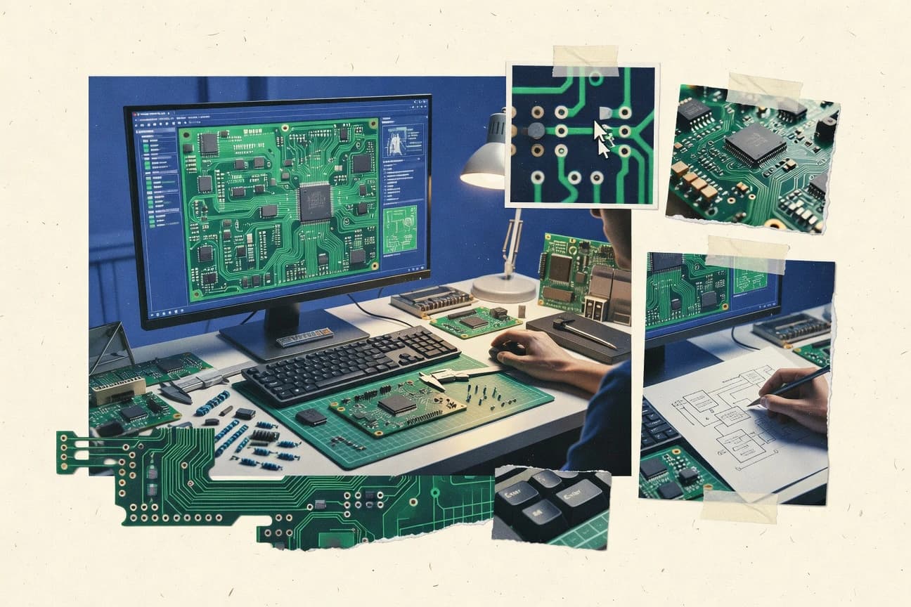
What Is Schematic Pcb Software?
Schematic PCB software combines schematic capture with PCB layout so nets, symbols, and component assignments flow from design intent into board geometry. It typically performs ERC for schematic wiring correctness and DRC for layout rule compliance before generating fabrication outputs like Gerbers and drill files. Altium Designer connects schematic-driven rules directly into PCB constraint checking, while KiCad ties schematic nets to PCB traces with bidirectional association that supports net syncing and rule checking.
Key Features to Look For
The right feature set determines whether schematic changes stay synchronized with PCB rules, routing, and manufacturing outputs.
Unified schematic-driven design rules with real-time constraint checking
Altium Designer provides unified schematic-driven PCB design rules and real-time constraint checking so net connectivity and constraints stay synchronized end to end. This reduces iteration time because rule violations can be caught as constraints propagate from schematic into PCB editing.
Schematic-to-PCB net connectivity linkage
Cadence OrCAD PCB Designer emphasizes net connectivity linkage from OrCAD Capture into PCB layout so schematic net and design object references remain consistent through board changes. EasyEDA also supports real-time schematic-to-layout net connectivity using generated netlists to reduce wiring and pin-mapping issues during handoff.
Bidirectional schematic and layout net association
KiCad provides bidirectional association between nets in the schematic and traces on the PCB so updates can be synchronized across design stages. This tight net association supports ERC and DRC workflows that catch both schematic and layout errors.
ERC and DRC rule checking tied to schematic intent
Altium Designer, KiCad, and Autodesk EAGLE all use ERC and DRC style validation to catch connectivity and clearance issues early. Proteus Design Suite focuses on simulation-driven schematic validation but it still supports schematic-first workflows that reduce the chance of committing faulty logic to layout.
Constraint-aware routing and adjustable auto-routing rules
Autodesk EAGLE stands out for its autorouter with adjustable rules so constraint-aware signal routing can be applied for multi-net boards. Altium Designer also supports powerful routing tools such as differential routing that aligns with complex stackups.
Manufacturing output generation from the same project assets
KiCad generates manufacturing outputs including Gerbers and drill files from its integrated schematic-to-PCB workflow. Autodesk EAGLE and EasyEDA similarly support common fabrication output exports so teams can move from capture and layout into PCB fabrication and assembly with fewer conversion steps.
How to Choose the Right Schematic Pcb Software
A practical selection process maps design workflow needs like rule rigor, schematic-to-layout synchronization, and output generation to tool capabilities.
Start with schematic-to-PCB synchronization requirements
Choose Altium Designer if the design process depends on unified schematic-driven PCB design rules and real-time constraint checking during PCB edits. Choose Cadence OrCAD PCB Designer if the team already uses OrCAD Capture and needs net connectivity continuity into PCB layout with constraint-driven editing.
Verify rule checking depth against the real failure modes
Select KiCad when ERC and DRC rule checking must be tied to schematic-to-layout net association so wiring mistakes and layout violations are both caught. Select Autodesk EAGLE when rule-based DRC and ERC style validation plus an autorouter with adjustable rules is needed for first-pass routing.
Match routing complexity and stackup needs to routing capability
Pick Altium Designer for rigid-flex and robust differential routing tools that support complex stackups. Pick Autodesk EAGLE when constraint-controlled autorouting with adjustable rules is the preferred path to faster signal routing.
Decide whether simulation should drive schematic iteration
Choose Proteus Design Suite when mixed-signal and digital logic verification must be tied to schematic-driven SPICE and logic models. Choose Tinkercad Circuits when fast circuit simulation inside a visual wiring workspace is the priority over production-grade schematic and PCB depth.
Align library and component workflow with the team’s handoff model
Select SPB/Altium Designer Auto-generated Libraries if the workflow centers on importing verified symbol and footprint pairs into Altium to reduce manual transcription effort. Choose EasyEDA when browser-based schematic-to-PCB work needs tight linking of symbols to footprints to prevent schematic and PCB mismatches.
Who Needs Schematic Pcb Software?
Schematic PCB software is used by teams that must transform electrical design intent into routed boards with rule checking and fabrication-ready exports.
Electronics teams building high-complexity schematic-to-PCB designs with rigorous rule checking
Altium Designer fits this segment because unified schematic-driven PCB design rules provide real-time constraint checking tied to schematic intent. It also supports advanced routing and rigid-flex design tools that align with complex board stackups.
Teams already using OrCAD Capture who need schematic-to-layout traceability
Cadence OrCAD PCB Designer fits teams that prioritize OrCAD Capture to PCB Designer net connectivity linkage for schematic-to-layout consistency. Its constraint-driven PCB editing supports consistent rule application during placement and routing changes.
Hardware teams needing full schematic-to-PCB design with strong rule checking and manufacturing outputs
KiCad fits teams that require integrated schematic capture plus PCB layout with ERC and DRC workflows. It generates Gerbers and drill files from the same project structure and supports bidirectional schematic-to-layout net syncing.
Learners and makers who need quick schematic validation with simulation
Tinkercad Circuits fits this segment because circuit simulation runs directly inside the visual wiring workspace. It enables rapid concept testing through schematic-style wiring and immediate visual feedback.
Common Mistakes to Avoid
Common buying mistakes come from underestimating synchronization, library discipline, and workflow depth gaps between tool types.
Choosing a tool that lacks real schematic-to-layout net synchronization
Tools like KiCad and EasyEDA provide schematic-to-layout net connectivity via bidirectional association or generated netlists, which prevents silent wiring and pin-mapping drift. Tools that act as companion utilities instead of full ECAD engines, like nRF Connect for Desktop, do not provide dedicated schematic capture and PCB layout engines for real design work.
Overlooking rule-checking requirements until late layout stages
KiCad and Altium Designer tie ERC and DRC workflows to schematic-to-layout net association so electrical and physical errors are caught early. Autodesk EAGLE also uses ERC and DRC style validation, but its constraint setup for routing requires careful rule discipline to avoid late surprises.
Under-planning library and constraint management on large projects
Altium Designer and Cadence OrCAD PCB Designer both require disciplined library and constraint setup because large complex projects can become heavy or need tuning. KiCad can slow down on large projects under heavy editing and DRC, so footprint and symbol workflows must be managed carefully.
Picking simulation-first tools for production-grade PCB schematic capture
Proteus Design Suite excels at executable simulation validation using schematic-driven SPICE and logic models, but its advanced PCB feature depth is less deep than specialized layout-centric CAD tools. Tinkercad Circuits provides circuit simulation and beginner workflows, but its export and integration into professional PCB toolchains are constrained for real production designs.
How We Selected and Ranked These Tools
We evaluated every tool on three sub-dimensions with fixed weights. Features carry 0.4 of the overall score, ease of use carries 0.3, and value carries 0.3. The overall rating is the weighted average computed as overall = 0.40 × features + 0.30 × ease of use + 0.30 × value. Altium Designer separated itself from lower-ranked tools with a concrete example on the features dimension because unified schematic-driven PCB design rules deliver real-time constraint checking that keeps schematic intent and PCB constraints synchronized.
Frequently Asked Questions About Schematic Pcb Software
Which schematic-to-PCB workflow has the strongest shared design intelligence?
What tool best preserves net connectivity from schematic entry through board editing?
Which option is best for running simulation-driven validation while iterating schematic changes?
Which software generates manufacturing outputs directly from schematic-connected projects?
Which tool is best for teams that want automation-friendly library management for Altium projects?
Which schematic and PCB workflow works best in a browser-first environment?
Which option supports rigid-flex board design with interactive routing backed by schematic-driven rules?
Which software is most suitable for digital and mixed-signal boards where co-simulation matters?
What tool choice fits Nordic embedded teams that need hardware bring-up around existing schematic work?
Tools reviewed
Primary sources checked during evaluation.
Referenced in the comparison table and product reviews above.
Keep exploring
Comparing two specific tools?
Software Alternatives
See head-to-head software comparisons with feature breakdowns, pricing, and our recommendation for each use case.
Explore software alternatives→In this category
Manufacturing Engineering alternatives
See side-by-side comparisons of manufacturing engineering tools and pick the right one for your stack.
Compare manufacturing engineering tools→FOR SOFTWARE VENDORS
Not on this list? Let’s fix that.
Our best-of pages are how many teams discover and compare tools in this space. If you think your product belongs in this lineup, we’d like to hear from you—we’ll walk you through fit and what an editorial entry looks like.
Apply for a ListingWHAT THIS INCLUDES
Where buyers compare
Readers come to these pages to shortlist software—your product shows up in that moment, not in a random sidebar.
Editorial write-up
We describe your product in our own words and check the facts before anything goes live.
On-page brand presence
You appear in the roundup the same way as other tools we cover: name, positioning, and a clear next step for readers who want to learn more.
Kept up to date
We refresh lists on a regular rhythm so the category page stays useful as products and pricing change.