GITNUXSOFTWARE ADVICE
Manufacturing EngineeringTop 10 Best Printed Circuit Board Software of 2026
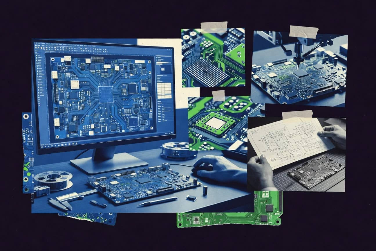
Discover the top 10 printed circuit board software tools to streamline your design process. Find the best solutions for efficient PCB creation here.

How we ranked these tools
Core product claims cross-referenced against official documentation, changelogs, and independent technical reviews.
Analyzed video reviews and hundreds of written evaluations to capture real-world user experiences with each tool.
AI persona simulations modeled how different user types would experience each tool across common use cases and workflows.
Final rankings reviewed and approved by our editorial team with authority to override AI-generated scores based on domain expertise.
Score: Features 40% · Ease 30% · Value 30%
Gitnux may earn a commission through links on this page — this does not influence rankings. Editorial policy
Editor’s top 3 picks
Three quick recommendations before you dive into the full comparison below — each one leads on a different dimension.
Altium Designer
Altium Designer DXP integrated environment with constraint-based PCB design and managed connectivity between views
Built for professional PCB design teams needing high-end constraints, automation, and manufacturing outputs.
Autodesk Fusion Electronics
Editor pick3D board and assembly context linking PCB layout to mechanical enclosure geometry
Built for teams integrating PCB design with 3D mechanical context for product-ready releases.
KiCad
Editor pick3D Viewer with accurate footprint visualization for geometry and clearance checks
Built for teams needing complete PCB design workflow with customizable rules.
Related reading
Comparison Table
This comparison table evaluates major printed circuit board design tools, including Altium Designer, Autodesk Fusion Electronics, KiCad, and OrCAD / PSpice, along with Cadence Allegro PCB Designer and other widely used packages. It summarizes how each option supports schematic capture, PCB layout, simulation and verification workflows, and manufacturing-ready output so teams can match the right tool to their requirements.
Altium Designer
PCB CADCreates schematics and PCB layouts with rules-driven design, 3D visualization, and fabrication outputs for manufacturing engineering workflows.
Altium Designer DXP integrated environment with constraint-based PCB design and managed connectivity between views
Altium Designer stands out with a unified design environment that tightly connects schematic capture, PCB layout, and rules-driven implementation. It delivers robust PCB capabilities such as constraint management, advanced routing tools, and high-fidelity signal integrity planning workflows.
Complex assemblies are handled through hierarchy-aware project management and integrated library handling, which reduces friction when iterating across many variants. The tool also supports manufacturing-facing outputs with clear design-for-manufacturing checks and comprehensive documentation generation.
- +Rules-driven design checks catch net, clearance, and constraint violations early
- +Advanced routing and constraint management reduce manual cleanup on complex boards
- +Tight schematic-to-layout synchronization keeps connectivity consistent across revisions
- +Strong library and hierarchy workflows support scalable multi-board and variant projects
- –Workspace customization can feel heavy for first-time users
- –Learning curve rises quickly due to dense feature depth across domains
- –Simulation and analysis workflows require deliberate setup for reliable results
- –Performance can degrade on very large projects with many connected documents
Best for: Professional PCB design teams needing high-end constraints, automation, and manufacturing outputs
More related reading
Autodesk Fusion Electronics
CAD suiteDesigns PCB schematics and layouts with integrated electronics libraries and manufacturing-ready exports in a Fusion-based workflow.
3D board and assembly context linking PCB layout to mechanical enclosure geometry
Autodesk Fusion Electronics stands out by combining PCB design workflows with full 3D product context so board geometry aligns with enclosure and mechanical parts. It supports schematic capture and layout for routing, component placement, and manufacturing outputs.
The tool also enables electronics-to-mechanical coordination through a shared model environment, which reduces rework during mechanical revisions. Collaboration and change management are supported through cloud-based project workflows.
- +Tight 3D board-in-context workflow for enclosure and mechanical fit checks
- +Unified schematic and PCB layout pipeline with consistent design data
- +Strong export support for manufacturing deliverables and documentation
- –Advanced routing and constraint workflows feel less streamlined than dedicated PCB suites
- –3D model management can add overhead during early layout iterations
- –Learning curve increases when mixing mechanical edits with electronics changes
Best for: Teams integrating PCB design with 3D mechanical context for product-ready releases
KiCad
open-sourceBuilds PCB projects from schematics to PCB layout with DRC, footprints, and Gerber and drill file generation for fabrication.
3D Viewer with accurate footprint visualization for geometry and clearance checks
KiCad stands out with a fully open-source EDA workflow that spans schematic capture, PCB layout, and engineering data management in one toolchain. It provides autorouting, DRC checking, and a 3D viewer to validate footprints and board stackups while iterating layouts. Libraries support symbol and footprint editing, and projects can use hierarchical sheets and net connectivity rules for larger designs.
- +Integrated schematic and PCB layout with direct net connectivity validation
- +Strong DRC with constraint-driven rule checks for clear layout correctness
- +Autorouter plus manual routing tools for flexible PCB implementation
- –Steep learning curve for advanced rules, footprints, and editing workflows
- –Complex projects can feel slower during large-library and constraint updates
- –Some advanced CAD workflows need add-ons or careful manual setup
Best for: Teams needing complete PCB design workflow with customizable rules
OrCAD / PSpice (Cadence Allegro PCB Designer)
enterprise EDAPerforms schematic capture and high-end PCB layout with advanced constraint checking and manufacturing file support for complex designs.
Constraint-driven routing and comprehensive DRC in Allegro PCB Designer
OrCAD and PSpice from Cadence focus on circuit design and simulation, while the OrCAD PCB flow connects tightly into PCB layout tasks in Allegro-based workflows. Cadence Allegro PCB Designer provides advanced schematic-to-layout integration, constraint-driven routing, and robust DRC for manufacturing-ready outputs.
PSpice supports detailed electrical verification that complements physical design decisions during layout iterations. Together, the suite targets teams that want simulation-backed PCB development rather than layout-only tooling.
- +Tight schematic-to-PCB integration with constraint mapping for fewer manual steps
- +Allegro-driven constraint routing supports complex nets and design rules
- +Strong DRC coverage for impedance, clearance, and manufacturing constraints
- +PSpice simulation enables electrical verification during PCB iteration
- –Training overhead is high due to dense configuration and rule setup
- –UI and workflows feel heavy for small projects and quick edits
- –Simulator and layout tools require coordination of libraries and models
- –Hardware capacity can limit performance on very large designs
Best for: Hardware teams using simulation-backed PCB design and Allegro-level DRC
Cadence Allegro PCB Designer
enterprise PCBImplements large-scale PCB routing and design management with constraint-driven editing and fabrication documentation outputs.
Constraint Manager with comprehensive DRC and netclass enforcement
Cadence Allegro PCB Designer stands out for deep, industrial-grade capabilities that support large-scale board design workflows. The software provides full schematic-to-layout processes with advanced routing, constraint-driven design checks, and extensive support for complex package and interconnect requirements.
It also emphasizes signal integrity readiness through simulation interfaces and comprehensive rule checking that targets manufacturing robustness. Design teams typically choose Allegro for repeatable engineering processes that scale across multi-board programs and high pin-count hardware.
- +Constraint-driven rule checking catches layout violations before release
- +Advanced routing supports complex nets and high pin-count board topologies
- +Robust support for complex packages, footprints, and manufacturing data
- –Steep learning curve due to dense feature set and workflow complexity
- –Interface and customization require training to maintain productivity
Best for: Large teams needing high-end PCB layout with strong verification and automation
EAGLE
PCB CADDesigns PCB layouts with integrated libraries, automated placement tools, and fabrication output generation for board manufacturing.
Rule-based Design Rules Check with immediate net and geometry feedback during layout
EAGLE stands out for its tightly integrated PCB design workflow and component-to-layout organization built around schematics. It supports schematic capture, PCB layout with interactive routing, rule-based design checks, and copper pour tools for faster board fills. The tool also emphasizes a mature parts-library ecosystem and extensibility through scripting and custom libraries for repeatable design patterns.
- +Integrated schematic-to-PCB workflow reduces manual net and footprint mapping
- +Rule-based design checks catch clearance, connectivity, and constraint issues early
- +Interactive routing and pour tools speed up typical two-layer layout tasks
- +Extensible libraries and scripting support repeatable component and footprint workflows
- –Advanced constraint handling for complex high-density routing can feel limiting
- –Large designs strain responsiveness compared with newer CAD workflows
- –3D visualization and mechanical integration are less central than in top-tier systems
- –Library management requires discipline to avoid footprint and naming inconsistencies
Best for: Small to mid-size teams doing practical schematic-to-board PCB work
Specctra (SPECTRA PCB Routing)
routing enginePerforms interactive and autorouting for PCB design with constraint handling and outputs to support fabrication workflows.
SPECCTRA autorouting using routing constraints and optimization strategies for controlled closure
Specctra SPECTRA PCB Routing stands out for its mature, constraint-driven autorouter workflow inside Mentor design environments. It supports detailed interactive routing with grid-based editing, connectivity preservation, and classic PCB operations like via placement and net class handling.
The software emphasizes high-routing quality for complex boards through controlled routing strategies, rule checking, and optimization loops. It is best assessed as an advanced routing engine rather than an all-in-one schematic and PCB design suite.
- +Constraint-based autorouting yields consistent results on high-density designs
- +Interactive routing keeps full control over nets, channels, and layer changes
- +Strong rule checking supports manufacturability-focused cleanup passes
- +Batch and strategy-driven optimization help converge on better routing outcomes
- –Routing strategy setup requires expertise to avoid poor first passes
- –Workflow is less intuitive than newer router-first GUI tools
- –Topology-heavy boards can demand multiple optimization cycles
- –Learning curve slows teams without prior CAD routing experience
Best for: Teams needing high-quality constraint routing in Mentor PCB workflows
Zuken CR-8000
industrial PCBManages schematic and PCB design data with rule checking and documentation outputs for manufacturing engineering coordination.
Library and rule management for BOM, footprints, and design constraints
Zuken CR-8000 stands out for its engineering data management around PCB libraries, rules, and netlist driven workflows across design and documentation. The tool supports schema to PCB handoff, constraint management, and rule checking tied to engineering objects like nets, components, and footprints.
It also emphasizes structured release and revision control for boards and documents, which helps traceability during change cycles. CR-8000 fits teams that want formal design governance rather than purely point-to-point editing.
- +Strong engineering data governance for nets, components, footprints, and rules
- +Good fit for schema to PCB change control with structured release management
- +Rule checking centered on design objects improves consistency across revisions
- –Steeper setup effort due to rule and library configuration requirements
- –Workflow depends heavily on correct object mapping and controlled library data
- –Limited appeal for ad hoc editing compared with lighter PCB utilities
Best for: Mid-size PCB teams needing controlled libraries, rules, and traceable design releases
PADS Professional
enterprise PCBSupports PCB schematic-to-layout flows with design rule checking and manufacturing output generation for production engineering.
Constraint-driven design rule checking across schematic and PCB domains
PADS Professional stands out for its mature PCB design workflow that emphasizes structured constraint-driven design from schematic to layout. It supports full ECAD tasks including schematic capture, PCB layout, routing, and rule checking with component and design constraints. The environment integrates with CAM outputs for fabrication and includes tools for documentation generation from the PCB database.
- +Constraint-based design workflow with robust ERC and DRC checks
- +Integrated schematic to PCB layout workflow with shared database
- +Strong CAM and documentation support for fabrication deliverables
- –Complex toolset creates a steep learning curve for new users
- –UI density slows navigation compared with more modern ECAD interfaces
- –Advanced automation often requires careful configuration and methodology
Best for: Teams needing constraint-driven PCB design with established ECAD workflows
PowerPCB (Allegro Alternatives Suite)
EDA suitePerforms PCB layout and routing with connectivity-driven editing and manufacturing outputs for board fabrication workflows.
Constraint-driven DRC that enforces design rules during iterative layout and edits
PowerPCB targets Allegro-style PCB design workflows and bundles them into an alternatives suite for schematic-to-layout engineering. It emphasizes layout capabilities like copper routing, stackup management, constraint-driven design checks, and manufacturing data preparation.
The tool is designed around EDA familiarity, using command patterns and workflows that reduce retraining for teams already built around Allegro-style processes. It is strongest when design rules and repeatable physical design flows matter more than novel, beginner-first interactivity.
- +Allegro-style workflow reduces retraining for existing physical design teams
- +Constraint-driven DRC supports systematic rule enforcement across design changes
- +Solid manufacturing outputs for fabrication and assembly documentation
- –Steeper learning curve than beginner-focused PCB tools
- –Advanced layout operations can feel interface-heavy without extensive practice
- –Integration breadth for niche third-party flows depends on project setup
Best for: Teams migrating Allegro-style PCB workflows needing efficient layout and checks
Conclusion
After evaluating 10 manufacturing engineering, Altium Designer stands out as our overall top pick — it scored highest across our combined criteria of features, ease of use, and value, which is why it sits at #1 in the rankings above.
Use the comparison table and detailed reviews above to validate the fit against your own requirements before committing to a tool.
How to Choose the Right Printed Circuit Board Software
This buyer’s guide explains what printed circuit board software must deliver across schematic capture, PCB layout, rule checks, routing, and fabrication outputs. It covers Altium Designer, Autodesk Fusion Electronics, KiCad, OrCAD and PSpice, Cadence Allegro PCB Designer, EAGLE, Specctra SPECTRA PCB Routing, Zuken CR-8000, PADS Professional, and PowerPCB. The guide maps concrete tool strengths to real design workflows such as constraint-driven release readiness and 3D enclosure-aligned layout.
What Is Printed Circuit Board Software?
Printed circuit board software is the ECAD toolchain used to create PCB schematics, place components, route nets, check manufacturing constraints, and generate fabrication deliverables. It solves connectivity consistency problems between schematic and layout, and it reduces release errors through rule checking, DRC, and constraint management. Tools like Altium Designer connect schematic-to-layout connectivity with constraint-based design checks and manufacturing output tooling. KiCad covers a complete schematic-to-PCB workflow with DRC, autorouting, and Gerber and drill generation for fabrication.
Key Features to Look For
The fastest way to choose PCB software is to match required deliverables and verification depth to the features each tool provides.
Rules-driven constraint checking that catches violations early
Altium Designer uses rules-driven design checks to catch net, clearance, and constraint violations early, which reduces late-stage cleanup on complex boards. EAGLE provides a rule-based Design Rules Check with immediate net and geometry feedback during layout for fast iteration.
Tight schematic-to-layout connectivity synchronization
Altium Designer keeps tight schematic-to-layout synchronization so connectivity stays consistent across revisions. EAGLE also uses an integrated schematic-to-PCB workflow that reduces manual net and footprint mapping effort.
Constraint-driven routing and controlled closure workflows
Specctra SPECTRA PCB Routing focuses on constraint-based autorouting using routing constraints and strategy-driven optimization for consistent results on high-density designs. Cadence Allegro PCB Designer emphasizes constraint-driven routing and uses a Constraint Manager with comprehensive DRC and netclass enforcement for repeatable closure.
Comprehensive DRC coverage aligned to manufacturing needs
Cadence Allegro PCB Designer provides comprehensive DRC coverage for manufacturing robustness and netclass enforcement through its Constraint Manager. OrCAD / PSpice pairs Allegro-based PCB routing with constraint-driven routing and robust DRC coverage for impedance, clearance, and manufacturing constraints.
3D context for geometry, enclosure fit, and clearance validation
Autodesk Fusion Electronics links PCB layout to enclosure geometry through a 3D board and assembly context workflow. KiCad includes a 3D Viewer that validates footprint visualization for geometry and clearance checks during layout iteration.
Library and revision governance for traceable releases
Zuken CR-8000 provides library and rule management tied to BOM, footprints, and design constraints, with structured release and revision control for change traceability. PADS Professional also emphasizes a constraint-driven design workflow with integrated schematic and PCB layout using a shared database to support consistent ECAD-to-fabrication deliverables.
How to Choose the Right Printed Circuit Board Software
Selection should start from the required workflow outcomes, then narrow to tools that match those outcomes with the specific feature depth they provide.
Define the release deliverables and verification depth
If manufacturing-ready outputs and robust constraint enforcement drive the workflow, Altium Designer supports fabrication documentation tooling plus drill and paste-ready documentation aligned to rule checking. If the workflow depends on Allegro-level DRC and netclass enforcement, choose Cadence Allegro PCB Designer because it centers verification through constraint management and comprehensive DRC.
Match routing strategy needs to the tool’s routing model
For teams that want autorouting quality under explicit constraints, Specctra SPECTRA PCB Routing provides constraint-based autorouting with batch and strategy-driven optimization loops. For teams needing industrial-grade constraint-driven routing inside a larger PCB environment, Cadence Allegro PCB Designer supports advanced routing and constraint-driven design checks for complex nets and high pin-count boards.
Decide how critical 3D enclosure context is to layout success
If mechanical enclosure fit checks are required during PCB layout, Autodesk Fusion Electronics links the PCB to mechanical enclosure geometry using a shared 3D product context workflow. If 3D geometry inspection is needed primarily for footprint validity and clearance checking, KiCad’s 3D Viewer enables iterative validation with accurate footprint visualization.
Evaluate library discipline and change control requirements
For organizations that require traceable design releases with controlled libraries and rule governance, Zuken CR-8000 manages engineering objects such as nets, components, and footprints and supports structured release and revision control. For teams using schematic-to-layout workflows with shared database consistency, PADS Professional emphasizes a constraint-driven design workflow with rule checking across schematic and PCB domains.
Choose the tool that fits the team’s training and workflow maturity
If a dense, feature-rich environment is acceptable and constraint automation is needed, Altium Designer can scale through hierarchy-aware project management and managed library workflows for multi-board and variant projects. If a routing-focused engine inside Mentor flows is the priority, Specctra SPECTRA PCB Routing provides a mature constraint-driven autorouter experience even though routing strategy setup requires expertise.
Who Needs Printed Circuit Board Software?
Printed circuit board software benefits hardware and electronics teams that must convert schematics into manufacturable, rules-verified PCB designs.
Professional PCB design teams that need high-end constraints and manufacturing outputs
Altium Designer fits these teams because it provides rules-driven design checks, advanced routing and constraint management, and comprehensive manufacturing outputs including drill and paste documentation tooling. Cadence Allegro PCB Designer also fits because its Constraint Manager enforces netclass rules with comprehensive DRC for industrial-grade verification.
Product teams that must align PCB layout with enclosure and mechanical geometry
Autodesk Fusion Electronics is the best match for enclosure-aligned layout because it links PCB and assembly context to mechanical revisions through a shared model environment. Fusion-based board-in-context workflows reduce rework when mechanical changes affect board geometry and fit.
Teams that need complete, customizable PCB design workflow and strong DRC basics
KiCad supports full schematic-to-PCB design with DRC checking, footprints, autorouting, and Gerber and drill file generation for fabrication. Its 3D Viewer supports geometry and clearance validation during layout iteration, which helps teams manage footprint correctness without switching tools.
Engineering organizations that require constraint governance, traceable releases, and controlled libraries
Zuken CR-8000 fits teams that require library and rule management for BOM, footprints, and design constraints with structured release and revision control. PADS Professional also fits teams that run established ECAD workflows because it emphasizes a shared database with constraint-driven design rule checking across schematic and PCB domains.
Common Mistakes to Avoid
Common selection failures come from choosing the wrong balance of constraint depth, routing workflow fit, and governance tooling for the actual design process.
Choosing a tool that does not support the required rule enforcement model
Teams that need systematic constraint enforcement during iterative edits benefit from tools like Cadence Allegro PCB Designer with Constraint Manager netclass enforcement or PowerPCB with constraint-driven DRC that enforces design rules during layout edits. EAGLE can work for teams that want immediate net and geometry feedback through its rule-based Design Rules Check, but complex high-density constraint workflows can feel limiting.
Underestimating training time for dense configuration-driven workflows
OrCAD / PSpice and Cadence Allegro PCB Designer include heavy rule setup and dense configuration that creates high training overhead for new teams. Allegro-style workflows also require careful configuration in PowerPCB alternatives, which can slow productivity until routing and rule methodology are standardized.
Using 3D visualization only as a final check instead of a workflow component
Autodesk Fusion Electronics is built around 3D board and assembly context linking PCB to enclosure geometry, so relying on late-stage checks can lead to mechanical rework. KiCad’s 3D Viewer enables geometry and clearance validation during layout iteration, which prevents late footprint clearance surprises.
Over-picking a routing engine without the right routing strategy expertise
Specctra SPECTRA PCB Routing produces high-quality constraint routing, but routing strategy setup requires expertise to avoid poor first passes. If strategy-driven optimization is not supported by team process, topology-heavy boards can demand multiple optimization cycles in Specctra.
How We Selected and Ranked These Tools
We evaluated every tool on three sub-dimensions. Features have a weight of 0.4 because PCB design success depends on capabilities such as rules-driven constraint checking, DRC depth, routing control, 3D context, and fabrication outputs. Ease of use has a weight of 0.3 because teams must navigate dense schematic and layout workflows efficiently, including library editing and constraint configuration. Value has a weight of 0.3 because the balance between workflow coverage and practical productivity affects day-to-day throughput. The overall rating is a weighted average computed as overall = 0.40 × features + 0.30 × ease of use + 0.30 × value, and Altium Designer separated at the top by pairing high feature capability like DXP integrated constraint-based PCB design with rules-driven early violation detection and manufacturing output tooling.
Frequently Asked Questions About Printed Circuit Board Software
Which PCB software is best for teams that need constraint-driven design across schematic capture and layout?
What tool fits projects that must align PCB layout with a 3D mechanical enclosure and coordinate changes?
Which software is most appropriate when signal integrity planning and electrical verification must influence layout decisions?
What option is best for open-source workflows that still need schematic capture, PCB layout, and 3D validation?
Which tool is designed for large, repeatable board programs with strong automation and verification at scale?
How do users choose between an all-in-one PCB suite and an advanced routing engine?
Which PCB software is best suited to teams that need formal design governance, version control, and traceability across revisions?
What software helps automate verification and documentation generation from the PCB database for manufacturing outputs?
Which option works well for routing closure and high-quality constraints during complex board routing iterations?
What tool is useful when a team is already built around Allegro-style workflows and wants alternatives for schematic-to-layout engineering?
Tools reviewed
Primary sources checked during evaluation.
Referenced in the comparison table and product reviews above.
Keep exploring
Comparing two specific tools?
Software Alternatives
See head-to-head software comparisons with feature breakdowns, pricing, and our recommendation for each use case.
Explore software alternatives→In this category
Manufacturing Engineering alternatives
See side-by-side comparisons of manufacturing engineering tools and pick the right one for your stack.
Compare manufacturing engineering tools→FOR SOFTWARE VENDORS
Not on this list? Let’s fix that.
Our best-of pages are how many teams discover and compare tools in this space. If you think your product belongs in this lineup, we’d like to hear from you—we’ll walk you through fit and what an editorial entry looks like.
Apply for a ListingWHAT THIS INCLUDES
Where buyers compare
Readers come to these pages to shortlist software—your product shows up in that moment, not in a random sidebar.
Editorial write-up
We describe your product in our own words and check the facts before anything goes live.
On-page brand presence
You appear in the roundup the same way as other tools we cover: name, positioning, and a clear next step for readers who want to learn more.
Kept up to date
We refresh lists on a regular rhythm so the category page stays useful as products and pricing change.