GITNUXSOFTWARE ADVICE
Manufacturing EngineeringTop 10 Best Electronic Circuit Making Software of 2026
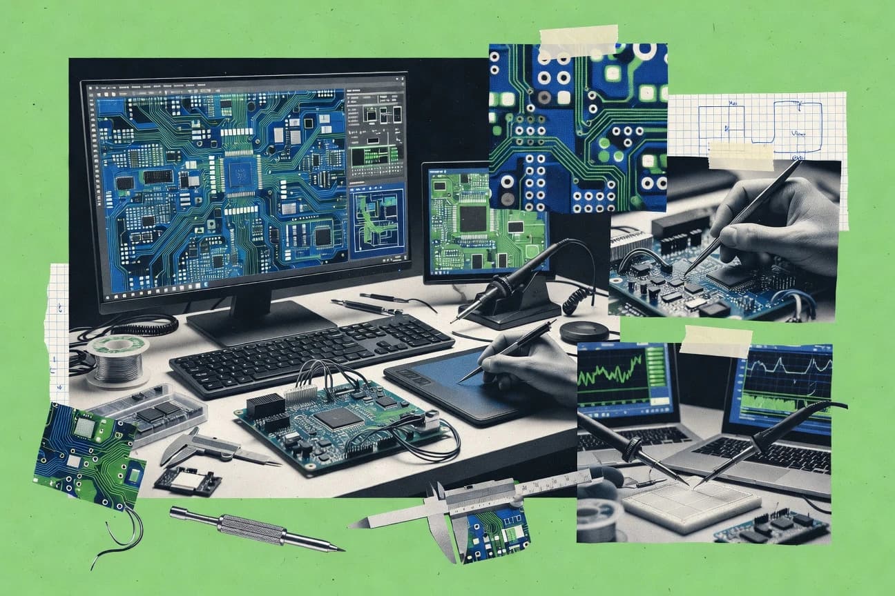
Explore the top 10 electronic circuit making software tools.

How we ranked these tools
Core product claims cross-referenced against official documentation, changelogs, and independent technical reviews.
Analyzed video reviews and hundreds of written evaluations to capture real-world user experiences with each tool.
AI persona simulations modeled how different user types would experience each tool across common use cases and workflows.
Final rankings reviewed and approved by our editorial team with authority to override AI-generated scores based on domain expertise.
Score: Features 40% · Ease 30% · Value 30%
Gitnux may earn a commission through links on this page — this does not influence rankings. Editorial policy
Editor’s top 3 picks
Three quick recommendations before you dive into the full comparison below — each one leads on a different dimension.
Autodesk Fusion 360
Electronics-to-mechanical integration for enclosure fit and design change coordination
Built for hardware teams needing CAD-linked PCB design and packaging validation.
Altium Designer
Editor pickConstraint-driven DRC tied to schematic and layout, enabling rule-based error prevention
Built for teams building complex PCB layouts needing automated checks and solid manufacturing output.
KiCad
Editor pickBoard-level DRC and fabrication-ready Gerber plus drill exports from the same design data
Built for indie to mid-size teams needing full PCB workflow without vendor lock-in.
Related reading
Comparison Table
This comparison table reviews electronic circuit making software used for schematic capture, PCB layout, and library management, including Autodesk Fusion 360, Altium Designer, KiCad, PADS Professional, and OrCAD. The entries focus on how each tool supports workflows, component ecosystems, and design constraints so readers can map features to project requirements.
Autodesk Fusion 360
electronics + CADCreates PCB schematics and routed electronic assemblies inside a unified CAD-CAM workflow that integrates mechanical design with electronic circuit modeling.
Electronics-to-mechanical integration for enclosure fit and design change coordination
Autodesk Fusion 360 stands out by unifying mechanical CAD, electronics workflow tooling, and simulation in one integrated environment. For electronic circuit making, it supports PCB design through its EDA integrations so users can place and route components with CAD-linked context.
It also enables electronics-to-mechanics considerations through shared models, which helps validate packaging fit alongside design changes. Fusion 360’s strength is coordinated product development rather than a standalone electronics-only drafting tool.
- +CAD and electronics work share context for enclosure and clearance checks
- +Integrated workflows reduce manual data transfer between mechanical and PCB stages
- +Supports iterative design with model-linked review for hardware-fit verification
- –Electronics tooling is less deep than dedicated PCB editors
- –Learning curve rises from combined CAD, electronics, and simulation workflows
- –Some electronics tasks depend on external EDA integrations
Best for: Hardware teams needing CAD-linked PCB design and packaging validation
More related reading
Altium Designer
pro PCB designDesigns electronic schematics and multi-layer PCBs with advanced libraries, signal integrity workflows, and manufacturing-ready output generation.
Constraint-driven DRC tied to schematic and layout, enabling rule-based error prevention
Altium Designer stands out for a unified, deeply integrated PCB design workflow that spans schematic capture, advanced PCB layout, and manufacturing data outputs. Its PCB editing is built around high-control routing, constraint-driven design checks, and library management that supports complex board development.
The tool also provides robust collaboration paths through project-based data organization and tight links from design intent to fabrication outputs. For electronic circuit making, it supports rigorous signal integrity and DRC-driven iteration across the full electronics-to-PBC pipeline.
- +Constraint-driven design rules catch schematic-to-PCB issues early
- +Advanced routing and interactive placement speed complex board iterations
- +Strong fabrication outputs with netlist-linked source of truth
- +Comprehensive library and component modeling for large designs
- –Steep learning curve for constraint, rule, and project configuration
- –Performance tuning can be needed for very large PCB projects
- –Tool flexibility can add setup overhead for small circuit boards
Best for: Teams building complex PCB layouts needing automated checks and solid manufacturing output
KiCad
open-source PCBGenerates circuit schematics and PCB layouts with open-source EDA tooling, including component symbol and footprint libraries.
Board-level DRC and fabrication-ready Gerber plus drill exports from the same design data
KiCad stands out for an open workflow that spans schematic capture, PCB layout, and manufacturing outputs in one toolchain. It supports hierarchical sheets, ERC rule checking, and symbol and footprint libraries tied to PCB footprints and fabrication layers.
KiCad generates Gerber, drill, and pick-and-place exports for typical PCB fabrication and assembly handoffs. It also includes 3D PCB visualization with interactive board and footprint inspection to catch mechanical fit issues early.
- +Integrated schematic, PCB layout, and manufacturing exports in one editor suite
- +Strong ERC and DRC support with configurable rules for project-specific constraints
- +3D viewer helps validate mechanical clearance and component placement before fabrication
- +Library system links symbols, footprints, and fabrication layer definitions
- +Gerber, drill, and centroid outputs cover common fabrication and assembly requirements
- –Learning curve is steeper than simpler single-purpose circuit tools
- –Large projects can feel slower during routing and complex rule checking
- –Editing and managing custom libraries takes careful discipline to avoid mismatches
- –Some advanced workflow automation requires more manual steps than code-based tools
Best for: Indie to mid-size teams needing full PCB workflow without vendor lock-in
PADS Professional
enterprise PCBCaptures schematics and performs PCB layout with design rule checks and outputs suitable for fabrication workflows.
Comprehensive design rule checking that enforces electrical and layout constraints across the PCB
PADS Professional stands out for a full PCB design workflow that spans schematic capture, simulation support, layout, and manufacturing document creation. The tool combines component and library management with rigid and flexible board design constraints, plus detailed rule checking for electrical and design-for-manufacturing readiness. Users get standard outputs like Gerber, drill, and assembly data from within the same environment to reduce translation steps.
- +End-to-end PCB workflow from schematic to layout and manufacturing outputs
- +Strong rule checking for design integrity and fewer fabrication re-spins
- +Library management supports disciplined component reuse across projects
- –Steeper learning curve than simpler editors for new CAD users
- –Advanced workflows require careful configuration of design rules and constraints
- –UI density can slow down iterative edits compared with lightweight tools
Best for: Teams needing full-featured PCB CAD with robust constraint and output support
OrCAD
schematic captureProduces electronic schematics and PCB artifacts with structured library management and manufacturing output support.
Rule-based DRC and constraint-driven PCB verification in the OrCAD PCB layout flow
OrCAD targets schematic capture and PCB design with a workflow built around Cadence’s OrCAD toolset. The suite supports hierarchical schematics, netlist-driven design handoff, and standard PCB layout tasks like routing and DRC for manufacturing readiness.
Integration with Cadence PCB and simulation ecosystems helps streamline verification and downstream analysis. Advanced users get control over design constraints and library content for complex board projects.
- +Strong schematic capture with hierarchical design support and net connectivity integrity checks
- +PCB layout includes constraint-driven workflows and rule-based design validation via DRC
- +Good library and data management support for repeatable board design practices
- –Toolchain complexity can slow setup for teams new to OrCAD workflows
- –Learning curve is steep for advanced constraint and rules configuration
- –Interoperability depends on correct netlist and data mapping between tools
Best for: Manufacturing-focused teams needing reliable PCB design rules and repeatable workflows
EAGLE
PCB editorCreates PCB layouts and schematic designs with an integrated library system and fabrication output workflows.
Design Rule Check enforcing clearances, widths, and manufacturing constraints
EAGLE from cadsoft.io stands out for a tight, integrated workflow between schematic capture and PCB layout in one desktop design environment. It supports standard circuit design flows with libraries, net connectivity, and design-rule checks to reduce layout-to-schematic mismatches.
Tight controls for layers, footprints, and routing enable practical board fabrication outputs with Gerber and drill exports. The tool also includes component and library management to keep symbols and footprints aligned across projects.
- +Integrated schematic-to-PCB workflow with connectivity-driven layout checks
- +Strong routing and layer stack controls for manufacturable PCB generation
- +Design-rule checks catch common geometry and clearance violations early
- +Reusable libraries for symbols, footprints, and consistent part selection
- –Editing and navigation can feel slower for large designs
- –Library management has a learning curve for maintaining custom footprints
- –Modern multi-user review and collaboration features are limited
Best for: Single-team hardware designers needing reliable PCB layout and DRC validation
EasyEDA
web-based PCBUses a browser-based editor to draw schematics and generate PCB layouts with shared libraries and export for fabrication.
Seamless schematic-to-PCB workflow inside the browser
EasyEDA stands out for turning schematic capture into a full PCB workflow inside one web interface. It supports circuit simulation, layout editing, and design rule checking to take designs from idea to manufacturable boards.
Library management and symbol and footprint creation help teams reuse parts across projects. The tool also integrates gerber and documentation outputs to streamline fabrication handoff.
- +Web-based schematic and PCB editor keeps workflows in one place
- +Integrated simulation and design rule checking reduces handoff mistakes
- +Large component library and quick symbol and footprint creation
- –Advanced PCB constraint workflows can feel limited versus desktop CAD
- –Library quality varies across community-contributed parts
- –Complex multi-sheet schematics need more careful organization
Best for: Students and small teams building and simulating PCB designs quickly
Proteus Design Suite
EDA + simulationDesigns schematic and PCB layouts and supports electronic simulation and verification for circuit designs.
Mixed-signal simulation with virtual instruments and co-simulation within Proteus
Proteus Design Suite stands out for combining schematic capture, PCB design, and circuit simulation in one workflow geared to electronics prototyping. Users can simulate analog, digital, and mixed-signal circuits with virtual instruments like oscilloscopes and logic analyzers. It also supports component libraries, hierarchical design, and measurement-oriented verification loops.
- +Integrated schematic-to-simulation workflow reduces verification handoff errors
- +Mixed-signal simulation with virtual instruments speeds debugging
- +Large component library and hierarchical design support complex projects
- –Simulation setup and instrumentation can feel heavyweight for quick checks
- –PCB workflow features feel less modern than dedicated layout tools
- –Learning curve is steeper for new users than single-purpose simulators
Best for: Designers verifying mixed-signal circuits with simulation-driven iteration
DipTrace
lightweight PCBDraws circuit schematics and creates PCB layouts with footprint management and design rule checks.
Integrated 3D PCB visualization with interactive review of component placement
DipTrace focuses on electronic circuit design with an integrated workflow that moves from schematic capture to PCB layout. The tool includes both 2D and 3D PCB visualization, plus library support for symbols, footprints, and components.
Design checks help catch connectivity and design-rule issues before manufacturing handoff. It is a strong fit for building real boards, not just documenting circuits.
- +Tight schematic-to-PCB workflow reduces handoff errors
- +3D PCB view helps verify clearances and mechanical fit
- +Automation tools for routing and placement speed typical board work
- +Design rule and connectivity checking catch issues before export
- +Component and footprint libraries support faster reuse
- –Advanced routing options can feel rigid compared with higher-end suites
- –Learning curve is noticeable for PCB editor workflow and constraints
- –Library management and parameterization require extra manual care
- –Some higher-end signal-integrity and simulation workflows are limited
Best for: Engineers designing small to mid-complexity PCBs with clear design checks
CircuitMaker
budget-friendly PCBGenerates schematics and PCBs with component libraries and export for manufacturing tasks.
Constraint-driven design rule checking during PCB layout
CircuitMaker stands out for combining schematic capture and PCB layout in a single workflow with a board-focused part library. The tool supports interactive routing and design rule checking to catch clearance and connectivity problems before fabrication. It also includes utilities for managing sheets, net connectivity, and typical PCB deliverables within the same project structure.
- +Tight schematic-to-PCB workflow with net connectivity continuity
- +Design rule checking highlights clearance and constraint issues early
- +Interactive routing speeds up trace placement compared with command-heavy tools
- –Schematic editor workflow feels less polished than top-tier competitors
- –Advanced constraint and simulation workflows require extra tooling
- –Library and footprint curation can be time-consuming for niche parts
Best for: Designers needing fast schematic-to-layout flow with practical DRC support
Conclusion
After evaluating 10 manufacturing engineering, Autodesk Fusion 360 stands out as our overall top pick — it scored highest across our combined criteria of features, ease of use, and value, which is why it sits at #1 in the rankings above.
Use the comparison table and detailed reviews above to validate the fit against your own requirements before committing to a tool.
How to Choose the Right Electronic Circuit Making Software
This buyer's guide covers how to choose electronic circuit making software across tools including Autodesk Fusion 360, Altium Designer, KiCad, PADS Professional, OrCAD, EAGLE, EasyEDA, Proteus Design Suite, DipTrace, and CircuitMaker. It connects real schematic capture, PCB layout, rule checking, simulation, and manufacturing export workflows to specific tool strengths and weaknesses. It also highlights common setup and workflow mistakes that repeatedly slow teams down across these options.
What Is Electronic Circuit Making Software?
Electronic circuit making software is the set of tools used to create schematics, lay out PCB traces and components, validate design rules, and generate manufacturing outputs like Gerber, drill, and assembly data. Many teams use these tools to reduce schematic-to-PCB mismatches by keeping net connectivity and design intent linked from capture through layout. Autodesk Fusion 360 supports CAD-linked PCB design and enclosure-fit validation in one integrated environment, while Altium Designer delivers constraint-driven DRC across schematic and layout with manufacturing-ready outputs. Proteus Design Suite extends circuit making with mixed-signal simulation using virtual instruments and co-simulation loops for verification before hardware moves forward.
Key Features to Look For
The right feature set depends on whether the workflow needs tight electronics-to-PCB manufacturability control, electronics-to-mechanics fit validation, or simulation-driven iteration.
Constraint-driven DRC and rule-based error prevention
Altium Designer excels at constraint-driven DRC tied to schematic and layout, which helps prevent rule-breaking issues from reaching fabrication. PADS Professional and OrCAD also emphasize comprehensive rule checking and DRC-style PCB verification to reduce electrical and layout re-spins.
Schematic-to-PCB net connectivity continuity
EAGLE, DipTrace, and CircuitMaker all focus on integrated schematic-to-PCB workflows that reduce handoff mistakes by enforcing connectivity and design-rule checks during layout. EasyEDA also keeps schematic-to-PCB inside a single browser interface so design intent travels with the board creation steps.
Fabrication and assembly export readiness from the same design source
KiCad generates manufacturing exports like Gerber, drill, and centroid outputs directly from board data so fabrication handoff stays consistent. Altium Designer and PADS Professional similarly emphasize fabrication outputs linked to netlist source of truth and rule checking for fewer translation steps.
Electronics-to-mechanics integration for enclosure and clearance validation
Autodesk Fusion 360 stands out by coordinating mechanical CAD and electronics workflow tooling so electronics changes can be verified against enclosure fit and clearance checks. This hardware-fit verification model-linked approach helps teams avoid mechanical packaging surprises when PCB routing evolves.
Mixed-signal and virtual-instrument simulation inside the circuit workflow
Proteus Design Suite is built for simulation-driven electronics iteration with mixed-signal simulation and virtual instruments like oscilloscopes and logic analyzers. This setup supports measurement-oriented verification loops that can shorten the path from schematic changes to validated behavior.
3D PCB visualization for mechanical clearance and placement inspection
DipTrace includes 3D PCB visualization with interactive review of component placement to validate clearances and mechanical fit early. KiCad also provides 3D PCB visualization for interactive inspection of board and footprint placement before fabrication.
How to Choose the Right Electronic Circuit Making Software
Picking the right tool comes down to mapping workflow needs like DRC depth, integration level, simulation requirement, and manufacturing output coverage to the specific strengths of each application.
Match the workflow integration level to the project’s constraints
Choose Autodesk Fusion 360 for projects that require CAD-linked PCB design and packaging validation with electronics-to-mechanical integration for enclosure fit and clearance checks. Choose Altium Designer when PCB build quality depends on constraint-driven DRC tied to schematic and layout with robust manufacturing-ready output generation. Choose KiCad when the priority is a full PCB workflow that includes schematic capture, PCB layout, and fabrication exports without vendor lock-in.
Prioritize rule checking that aligns with the errors that matter most
If the biggest risk is schematic-to-PCB rule violations, prioritize Altium Designer because its constraint-driven DRC catches schematic-to-PCB issues early. If the risk is both electrical integrity and design-for-manufacturing readiness, evaluate PADS Professional because it enforces electrical and layout constraints with detailed rule checking. If the risk is complex design rule verification repeatability, OrCAD’s rule-based DRC and constraint-driven PCB verification fit manufacturing-focused team workflows.
Confirm manufacturing output coverage from a single design dataset
If fabrication handoff consistency is the priority, evaluate KiCad because it outputs Gerber and drill along with fabrication and assembly requirements like centroid output. If manufacturing deliverables must stay tightly linked to design intent for complex boards, Altium Designer supports netlist-linked source of truth across design and fabrication outputs. If a tool needs to produce Gerber and drill exports from a tight schematic-to-PCB workflow, EAGLE supports layout-to-fabrication outputs while maintaining clearances, widths, and manufacturing constraints.
Add simulation only when verification requires it
Select Proteus Design Suite when mixed-signal simulation and virtual instruments like oscilloscopes and logic analyzers are required for debugging before committing to hardware iteration. For teams that mainly need PCB layout reliability and manufacturing outputs, focus on DRC and export workflows in Altium Designer, PADS Professional, and KiCad rather than simulator depth. If simulation is secondary and speed of schematic-to-layout delivery is more critical, EasyEDA and CircuitMaker keep the schematic-to-PCB path streamlined.
Plan for learning curve and scaling behavior based on team and design size
For large complex PCB layouts, Altium Designer can deliver advanced routing and interactive placement speed but it also has a steep learning curve for constraint and project configuration. KiCad and PADS Professional also involve learning curves from integrated workflows, and KiCad can feel slower on large projects during routing and complex rule checking. EAGLE and CircuitMaker tend to fit smaller, single-team board work where a simpler integrated flow is easier to adopt, while DipTrace adds 3D visualization for placement review with a noticeable learning curve for PCB editor workflow and constraint handling.
Who Needs Electronic Circuit Making Software?
Different teams need different combinations of schematic capture, PCB layout validation, simulation, and fabrication exports.
Hardware teams needing CAD-linked PCB design and packaging validation
Autodesk Fusion 360 is the best fit because electronics-to-mechanical integration supports enclosure fit and design change coordination through model-linked review. This segment benefits from preventing clearance and enclosure issues while PCB iterations continue.
Teams building complex PCB layouts that require automated checks and strong manufacturing output
Altium Designer is the top choice because constraint-driven DRC tied to schematic and layout helps prevent rule-based errors and it generates solid fabrication outputs. Teams that manage complex board development gain value from advanced libraries and netlist-linked source of truth.
Indie to mid-size teams that want full PCB workflow without vendor lock-in
KiCad is a strong match because it provides integrated schematic and PCB layout with ERC and configurable rule checking plus manufacturing exports like Gerber and drill. The 3D PCB viewer supports early mechanical clearance and component placement validation.
Designers verifying mixed-signal circuits with simulation-driven iteration
Proteus Design Suite fits this audience because it combines schematic-to-simulation with mixed-signal simulation and virtual instruments. Co-simulation and instrumentation-based debugging support faster verification loops for circuit behavior.
Common Mistakes to Avoid
Several recurring pitfalls across these tools come from mismatched workflow expectations, insufficient setup discipline, and assuming design rule checks are handled automatically without configuration effort.
Buying a CAD electronics tool but skipping enclosure fit validation
Teams that need packaging assurance should not rely only on PCB layout in tools that do not coordinate electronics-to-mechanics fit. Autodesk Fusion 360 specifically supports electronics-to-mechanical integration for enclosure fit and design change coordination to address this mismatch.
Underestimating the setup effort behind constraint and rule systems
Altium Designer can catch issues early with constraint-driven DRC, but it requires steep learning for constraint and project configuration. PADS Professional and OrCAD also rely on careful configuration of design rules and constraints, so rule setup time must be planned for successful use.
Assuming library quality will be consistent across community content
EasyEDA includes a large component library with quick symbol and footprint creation, but library quality varies across community-contributed parts. EAGLE, DipTrace, and CircuitMaker also require careful library and footprint curation for consistent part selection and fewer mismatches.
Choosing a simulation-centric workflow without validating PCB layout constraints
Proteus Design Suite helps verification using mixed-signal simulation and virtual instruments, but its PCB workflow features can feel less modern than dedicated layout tools. For hardware that must go to fabrication, pair simulation-driven design with strong PCB layout DRC in Altium Designer, KiCad, or PADS Professional to prevent clearance and rule violations.
How We Selected and Ranked These Tools
we evaluated each tool on three sub-dimensions: features with weight 0.4, ease of use with weight 0.3, and value with weight 0.3. The overall rating is the weighted average computed as overall = 0.40 × features + 0.30 × ease of use + 0.30 × value. Autodesk Fusion 360 separated itself from lower-ranked tools by delivering electronics-to-mechanical integration for enclosure fit and design change coordination, which directly strengthened the features score because it reduces mechanical clearance risk during hardware iteration.
Frequently Asked Questions About Electronic Circuit Making Software
Which tools provide an integrated schematic-to-PCB workflow without exporting data to a separate environment?
What software is best for PCB design teams that need constraint-driven rule checking tied to schematic intent?
Which option supports electronics-to-mechanics validation for enclosure fit and packaging constraints?
Which tools generate fabrication outputs like Gerber and drill in a way that supports real board handoff?
Which software is most suitable for mixed-signal verification using simulation and measurement-style instruments?
How do the top PCB tools compare for signal integrity validation and error prevention before manufacturing?
Which software supports library management and hierarchical schematics for larger projects?
What toolchain is most appropriate for teams that want vendor-neutral exports and minimal lock-in?
Which applications are strongest for rapid prototyping where schematic and PCB edits must happen quickly in one place?
Tools reviewed
Primary sources checked during evaluation.
Referenced in the comparison table and product reviews above.
Keep exploring
Comparing two specific tools?
Software Alternatives
See head-to-head software comparisons with feature breakdowns, pricing, and our recommendation for each use case.
Explore software alternatives→In this category
Manufacturing Engineering alternatives
See side-by-side comparisons of manufacturing engineering tools and pick the right one for your stack.
Compare manufacturing engineering tools→FOR SOFTWARE VENDORS
Not on this list? Let’s fix that.
Our best-of pages are how many teams discover and compare tools in this space. If you think your product belongs in this lineup, we’d like to hear from you—we’ll walk you through fit and what an editorial entry looks like.
Apply for a ListingWHAT THIS INCLUDES
Where buyers compare
Readers come to these pages to shortlist software—your product shows up in that moment, not in a random sidebar.
Editorial write-up
We describe your product in our own words and check the facts before anything goes live.
On-page brand presence
You appear in the roundup the same way as other tools we cover: name, positioning, and a clear next step for readers who want to learn more.
Kept up to date
We refresh lists on a regular rhythm so the category page stays useful as products and pricing change.