GITNUXSOFTWARE ADVICE
Manufacturing EngineeringTop 10 Best Ic Layout Software of 2026
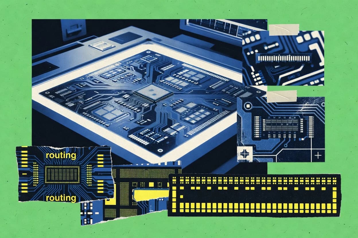
Compare the top Ic Layout Software tools with a ranked shortlist, covering Synopsys Custom Compiler, Siemens EDA, and Mentor PADS. Explore picks!

How we ranked these tools
Core product claims cross-referenced against official documentation, changelogs, and independent technical reviews.
Analyzed video reviews and hundreds of written evaluations to capture real-world user experiences with each tool.
AI persona simulations modeled how different user types would experience each tool across common use cases and workflows.
Final rankings reviewed and approved by our editorial team with authority to override AI-generated scores based on domain expertise.
Score: Features 40% · Ease 30% · Value 30%
Gitnux may earn a commission through links on this page — this does not influence rankings. Editorial policy
Editor’s top 3 picks
Three quick recommendations before you dive into the full comparison below — each one leads on a different dimension.
Synopsys Custom Compiler
Constraint-driven physical implementation that automates optimization for predictable signoff-ready layouts
Built for teams delivering production custom IC layouts needing predictable physical closure.
Siemens EDA (Tanner and custom IC flow)
Editor pickRule-driven DRC and verification in the custom IC layout flow
Built for custom IC teams needing rule-based layout control and mixed-flow compatibility.
Mentor Graphics PADS
Editor pickConstraint-based DRC tied to PCB layout to prevent clearances and spacing violations
Built for engineering teams needing production-focused PCB layout with rule-driven verification.
Related reading
Comparison Table
This comparison table evaluates IC layout and custom-design tooling across major ecosystems, including Synopsys Custom Compiler, Siemens EDA Tanner and custom IC flow, Mentor Graphics PADS, Altium Designer, and KiCad. It summarizes how each platform handles schematic-to-layout workflows, device and PDK integration, routing and verification stages, and the level of customization available for layout-centric design tasks.
Synopsys Custom Compiler
EDA custom ICCustom IC implementation and layout-centric design flow that supports standard cell assembly, routing, and physical closure steps for custom designs.
Constraint-driven physical implementation that automates optimization for predictable signoff-ready layouts
Synopsys Custom Compiler stands out for its tight integration with the Synopsys custom design flow and production-ready signoff support. The tool handles detailed cell and block implementation tasks like sizing, placement, routing, and extraction, targeting predictable physical results.
It also supports advanced automation through constraint-driven optimization and techfile-based manufacturing assumptions. Teams use it to move from RTL or schematic intent to finalized layout outcomes with consistent electrical-physical correlation.
- +Constraint-driven optimization improves layout quality across complex analog and digital blocks
- +Integrated extraction and signoff-oriented checks reduce physical and electrical mismatch
- +Strong techfile and PDK alignment supports reliable manufacturing assumptions
- +Automation accelerates iteration loops for timing, area, and manufacturability
- –Requires careful constraint setup to avoid nonconvergent optimization runs
- –Workflow complexity increases ramp-up for teams used to simpler layout tools
- –Signoff focus can add extra run steps even for early exploration
- –Debugging physical closure issues can require deep understanding of constraints
Best for: Teams delivering production custom IC layouts needing predictable physical closure
More related reading
Siemens EDA (Tanner and custom IC flow)
EDA custom ICCustom IC design and layout tooling within Siemens EDA offerings, including physical design and verification capabilities for integrated circuits.
Rule-driven DRC and verification in the custom IC layout flow
Siemens EDA stands out for supporting both Tanner-based design flows and Siemens custom IC layout methodologies in a single toolset. It provides layout creation and edit tools plus rule-driven verification to catch geometry and connectivity issues before tape-out.
The custom IC flow emphasizes systematic physical design tasks, including constraint handling, layout database management, and incremental implementation. It is a strong fit for organizations needing predictable physical design control for complex analog, mixed-signal, and custom digital blocks.
- +Custom IC layout tooling aligned with Siemens physical design constraints
- +Tanner-compatible flow support for mixed methodology design teams
- +Rule-driven verification helps detect layout and connectivity violations early
- –Workflow complexity can slow teams migrating from simpler layout tools
- –Tight integration expects strong database and process rule discipline
- –Toolchain learning curve is steeper than mainstream entry layout editors
Best for: Custom IC teams needing rule-based layout control and mixed-flow compatibility
Mentor Graphics PADS
board-layout EDAPCB-centric design environment that includes layout creation, rule checking, and manufacturing data output for electronic hardware related to IC systems.
Constraint-based DRC tied to PCB layout to prevent clearances and spacing violations
Mentor Graphics PADS stands out for its integrated PCB design workflow aimed at delivering production-ready layout deliverables. It supports multi-sheet schematic capture to netlist-driven PCB layout, plus routing, layer management, and constraint-based design checks.
The tool includes signal integrity and manufacturing data preparation functions that help teams align electrical design intent with fabrication outputs. PADS also supports library management for symbols and footprints to maintain consistency across projects and revisions.
- +Netlist-driven PCB layout keeps schematic connectivity consistent across the design flow
- +Constraint-driven design rule checks catch clearances, spacing, and topology issues early
- +Layer-aware routing supports complex stackups for board-level signal routing needs
- +Library management helps standardize footprints and component symbols across teams
- +Fabrication-output tooling streamlines generation of assembly and fabrication documentation
- –Large designs can feel slower during placement and route iterations
- –Advanced visualization options can lag behind modern interactive UX expectations
- –Some workflows require deeper setup of rules and constraints per project
- –Cross-probing between schematic and layout can be less seamless than top-tier tools
Best for: Engineering teams needing production-focused PCB layout with rule-driven verification
Altium Designer
board-layout EDAElectronics design platform with schematic and PCB layout tools plus fabrication output tooling for IC-linked hardware assemblies.
Integrated design rule checking with constraint-driven interactive routing and manufacturability verification
Altium Designer stands out for its deep ECAD to PCB workflow coverage, including schematic capture tightly linked to PCB design. The software supports multilayer PCB layout, interactive constraint-driven design, and robust DRC and rule checking for manufacturability.
It includes advanced routing tools such as interactive routing, push-and-shove behavior, and comprehensive signal integrity-oriented analysis workflows. The tool also supports rigid-flex and complex stackups with detailed fabrication and documentation outputs.
- +Tight schematic-to-PCB synchronization with constraint reuse across design changes
- +Powerful interactive routing with push-and-shove and fast net management
- +Advanced DRC and rule checking for electrical and manufacturability issues
- +Rich multilayer and rigid-flex stackup configuration for complex boards
- –Steep learning curve for constraint setup and advanced layout workflows
- –Resource-heavy projects can stress CPU and memory during editing
- –Dense interface can slow navigation for small single-board projects
- –Custom workflow automation requires deeper setup effort than basic editors
Best for: Design teams needing high-control multilayer and rigid-flex PCB layout workflows
KiCad
open-source ECADOpen-source ECAD suite that generates PCB footprints, runs design rule checks, and exports manufacturing files for IC-connected products.
Unified schematic and PCB workflow with netlist-driven DRC and cross-probing
KiCad stands out by combining schematic capture and PCB layout in one installable desktop application with open file formats. It supports a complete PCB workflow with netlist-driven design-rule checking, multilayer stackups, footprints, and interactive routing.
The tool includes robust annotation, footprint management, and simulation integration options so teams can validate electrical intent beyond just placement. KiCad also provides production outputs via Gerber, drill, and fabrication exports needed for manufacturing handoff.
- +Tight schematic-to-PCB sync via netlists and cross-probing
- +Strong design-rule checking with configurable electrical and geometry rules
- +Interactive autorouting with manual control over constraints
- –Complex project setup can feel heavy for small one-off boards
- –Some advanced layout automation requires careful rule tuning
- –Library quality varies and may need footprint auditing
Best for: Hobbyists and engineers building custom PCBs with full offline control
Autodesk EAGLE
ECAD layoutSchematic and PCB layout software with library management and fabrication export workflows used for electronic hardware integration.
Design Rule Check with rules-based clearance and constraint enforcement
Autodesk EAGLE stands out for a mature PCB workflow built around a schematic-to-layout flow and strong library management. It includes layout rules, design rule checks, and interactive routing tools to speed up board creation.
It supports component footprints, hierarchical schematics, and netlist-driven synchronization between schematic and board. It also integrates fabrication outputs like Gerber and drill exports for downstream manufacturing steps.
- +Schematic to board synchronization keeps nets consistent across edits
- +Design rule checks catch routing and clearance issues before export
- +Large parts and footprint libraries support common PCB component footprints
- +Interactive routing tools speed manual trace placement
- +Gerber and drill export formats support standard manufacturing workflows
- –Advanced automation depends on add-ons or scripting effort
- –Large projects can feel slower during editing and rule checking
- –Component data quality issues often appear when importing third-party libraries
- –3D visualization and mechanical integration are limited versus MCAD-focused tools
Best for: Designers needing reliable schematic-to-PCB flow for typical embedded hardware boards
Zuken CR-8000
design data managementEngineering design management and design integration tools used to control schematic and layout work for complex electronic systems tied to IC designs.
Automated design rules checking with constraint-driven routing guidance
Zuken CR-8000 stands out with automated rules checking and design management workflows aimed at keeping complex PCB layouts consistent. The software supports constraint-driven routing, component placement control, and schematic-to-layout data synchronization for reducing manual rework.
It also emphasizes multi-board and variant-aware layout practices that help teams reuse designs while maintaining electrical and mechanical constraints. CR-8000 fits organizations that need predictable compliance checks and controlled design change propagation across engineering releases.
- +Rules-driven design checks catch net, spacing, and constraint violations early
- +Schematic-to-layout synchronization reduces orphan nets and manual alignment work
- +Constraint-based routing improves consistency across complex board topologies
- +Variant and multi-board workflows support controlled reuse of design baselines
- –Automation requires accurate constraint setup to avoid noisy rule conflicts
- –Complex rule systems can slow onboarding for new layout engineers
- –GUI workflows can feel heavy for small boards and simple routing needs
Best for: Teams managing constraint-heavy PCB layouts with strict release control
Siemens EDA (IC Compiler flow)
physical-implementationAn integrated physical implementation toolchain for custom and standard-cell digital IC flows that targets layout closure and manufacturability checks.
Congestion-aware timing-driven optimization across place and detailed route phases
Siemens EDA’s IC Compiler flow stands out with a full physical implementation methodology that integrates seamlessly with standard Samsung and foundry design rules. The tool supports place and route with systematic timing closure, detailed routing, and signoff-oriented verification steps aligned to industry flows.
Designers get robust constraints handling for timing, congestion, and DRC-driven closure across large digital blocks. The workflow emphasizes predictable results through scripted run control, analysis reports, and iterative optimization loops.
- +Tight timing closure workflow for complex digital blocks and hard constraints
- +Integrated place and route with congestion-aware optimization steps
- +Strong DRC-driven physical closure support through foundry rule integration
- +Workflow automation via scripted run control and consistent output reporting
- –Steep learning curve for constraint setup and physical closure tuning
- –Verification output volume can be heavy for frequent iteration cycles
- –Physical-only focus can require separate flows for full signoff coverage
- –Less suited for very small designs that need minimal methodology overhead
Best for: Large ASIC teams needing repeatable physical implementation and closure workflows
Ansys HFSS
RF verificationA 3D electromagnetic field solver used to model RF components and verify performance that can be used to guide IC layout decisions for high-frequency structures.
Adaptive mesh refinement with accurate S-parameter and field extraction
Ansys HFSS stands out for full-wave electromagnetic simulation of microwave and RF hardware using accurate 3D finite element meshing. It supports co-simulation workflows through tight integration with circuit and system-level environments, which helps link component geometry to electrical performance.
The tool can model complex boundaries, material properties, and excitation types to predict S-parameters, resonance behavior, and field distributions for interconnects and packages. For IC layout workflows, it is most effective when layout-generated geometry is converted into simulation-ready models for high-frequency validation rather than for mask-level drafting.
- +Full-wave 3D EM solves capture complex field effects
- +Robust material and boundary condition modeling for RF accuracy
- +S-parameter and field results support detailed interconnect validation
- –Not designed for mask-level IC layout editing
- –Large 3D models can require significant compute and memory
- –Mesh setup and convergence tuning add setup overhead
Best for: RF and microwave teams simulating interconnects from layout-derived geometry
Keysight ADS
RF designA microwave and RF circuit design platform with device and EM co-simulation workflows that inform IC layout parameters for RF front-end design.
ADS layout and schematic integration with layout-driven electromagnetic validation
Keysight ADS distinguishes itself with tightly integrated RF and microwave circuit design workflows that connect schematic capture to planar and EM-aware layouts. The software supports detailed placement and routing for RF interconnects and enables layout-driven analysis through electromagnetic simulation workflows.
ADS also manages design intent using hierarchical schematic and layout links, which helps preserve connectivity across iterations. The tool is most useful when RF circuit architecture, layout geometry, and validation are part of one continuous environment.
- +Schematic-to-layout connectivity preserves nets across design iterations
- +Integrated EM simulation workflows support layout-driven validation
- +Hierarchical design reuse speeds updates of complex RF blocks
- +Strong routing and geometry tools for RF interconnect creation
- +Design rule support helps reduce fabrication-unfriendly geometries
- –Layout workflows can feel specialized compared with generic PCB tools
- –Complex EM setup can slow teams that need quick visual routing
- –Learning curve is steep for ADS-specific design management concepts
- –Large designs may tax system performance during simulation cycles
Best for: RF teams building EM-validated layouts inside a unified circuit workflow
How to Choose the Right Ic Layout Software
This buyer’s guide helps teams pick the right IC layout software tool by mapping concrete capabilities to real design workflows across Synopsys Custom Compiler, Siemens EDA custom IC flow, and IC Compiler flow. It also covers PCB-focused IC-linked workflows in Mentor Graphics PADS, Altium Designer, KiCad, Autodesk EAGLE, and Zuken CR-8000. RF-focused geometry and validation workflows are covered through Ansys HFSS and Keysight ADS.
What Is Ic Layout Software?
IC layout software creates and edits physical layouts for integrated circuits, then checks geometry and connectivity against rule sets for manufacturability and electrical intent. It solves problems like layout-vs-schematic mismatch, missing or conflicting constraints, and physical closure failures caused by congestion, DRC violations, or optimization that does not converge. Teams use it for custom analog and mixed-signal blocks, standard-cell or ASIC physical implementation, and RF interconnect validation where layout geometry drives performance. Examples include Synopsys Custom Compiler for constraint-driven custom physical implementation and Siemens EDA IC Compiler flow for congestion-aware timing-driven place and route closure.
Key Features to Look For
The right IC layout tool reduces physical and electrical mismatch by combining constraint-aware implementation with rule-driven verification and workflow automation.
Constraint-driven physical implementation and optimization
Synopsys Custom Compiler uses constraint-driven physical implementation that automates optimization for predictable signoff-ready layouts. Siemens EDA custom IC flow also emphasizes systematic constraint handling with rule-aligned layout control for complex analog and mixed-signal blocks.
Rule-driven DRC and verification tied to layout behavior
Siemens EDA custom IC flow provides rule-driven DRC and verification in the custom IC layout flow to detect geometry and connectivity violations before tape-out. Mentor Graphics PADS, Altium Designer, KiCad, and Autodesk EAGLE apply rule-driven design checks in PCB workflows that prevent clearances and routing topology errors that commonly break fabrication handoff.
Integrated extraction and signoff-oriented checks for electrical-physical correlation
Synopsys Custom Compiler integrates extraction and signoff-oriented checks to reduce electrical and physical mismatch during iteration. This is paired with techfile and PDK alignment so manufacturing assumptions stay consistent with physical outcomes.
Congestion-aware timing-driven place and route optimization for digital closure
Siemens EDA IC Compiler flow uses congestion-aware timing-driven optimization across place and detailed route phases for repeatable closure on large digital blocks. It combines DRC-driven physical closure support with constraints for timing, congestion, and physical rule correctness.
Schematic-to-layout connectivity synchronization with cross-probing
Altium Designer links schematic changes to PCB routing with constraint reuse and robust DRC for manufacturability. KiCad and Autodesk EAGLE also rely on netlist-driven synchronization and cross-probing to keep nets consistent across edits and reduce orphan-net problems.
Layout-driven RF or interconnect validation via EM simulation integration
Keysight ADS connects layout geometry to electromagnetic validation through integrated EM simulation workflows for RF front-end design. Ansys HFSS performs full-wave 3D EM solves with adaptive mesh refinement and extracts S-parameters and field results from models derived from layout geometry.
How to Choose the Right Ic Layout Software
Choosing the right tool starts with the physical scope needed, then maps to constraint automation, DRC verification strength, and how simulation or signoff requirements connect to layout.
Match tool scope to IC type and signoff expectations
For production custom IC layouts that require predictable physical closure, Synopsys Custom Compiler fits best because it supports constraint-driven physical implementation and integrates extraction and signoff-oriented checks. For custom IC work that needs rule-driven verification and mixed methodology compatibility, Siemens EDA custom IC flow targets rule-aligned layout control using Tanner-compatible flow support.
Select the verification approach that matches the risks in the workflow
If layout geometry and connectivity must be validated before tape-out, Siemens EDA custom IC flow uses rule-driven DRC and verification inside the custom IC layout flow. For IC-linked PCB deliverables where spacing and clearance violations drive rework, Mentor Graphics PADS and Altium Designer provide constraint-based DRC and interactive routing paired with manufacturability rule checking.
Choose a constraint and optimization model that will converge in real projects
Synopsys Custom Compiler can accelerate iteration loops for timing, area, and manufacturability using constraint-driven optimization, but it requires careful constraint setup to avoid nonconvergent runs. Siemens EDA IC Compiler flow also has steep constraint setup and physical closure tuning requirements, but it focuses on congestion-aware timing-driven optimization that improves repeatability for large ASIC blocks.
Pick a workflow synchronization model that prevents mismatch work
When electrical connectivity must remain consistent through edits, Altium Designer uses tight schematic-to-PCB synchronization with constraint reuse. KiCad and Autodesk EAGLE also use netlist-driven DRC and synchronization so routing edits align with schematic connectivity across complex PCB layers.
Add EM validation only if RF geometry and performance are in scope
For RF interconnect and microwave structures where layout-derived geometry must be simulated, Ansys HFSS provides full-wave 3D EM solves with adaptive mesh refinement and accurate S-parameter and field extraction. For RF front-end workflows that keep schematic-to-layout links inside one environment, Keysight ADS connects placement and routing to integrated EM simulation for layout-driven validation.
Who Needs Ic Layout Software?
IC layout software benefits teams whose deliverables require physical correctness against rule sets, electrical correlation, and closure targets, plus optional RF simulation validation.
Production custom IC teams that need predictable physical closure
Synopsys Custom Compiler is the primary fit for production custom IC layouts because it automates constraint-driven optimization and includes integrated extraction and signoff-oriented checks that reduce electrical-physical mismatch. Siemens EDA custom IC flow also supports rule-driven DRC and verification with mixed-flow compatibility for custom IC groups that want systematic physical design control.
Large ASIC teams focused on repeatable physical implementation and closure
Siemens EDA IC Compiler flow is built for large ASIC physical implementation by combining congestion-aware timing-driven optimization with DRC-driven physical closure support. This matches teams that need systematic scripted run control, iterative optimization loops, and consistent output reporting across place and detailed route.
Engineering teams shipping production PCB layouts for IC systems
Mentor Graphics PADS is designed for production-focused PCB layout with constraint-based DRC that prevents clearance and spacing violations. Altium Designer targets high-control multilayer and rigid-flex PCB layout with interactive constraint-driven routing and manufacturability verification.
RF teams that validate interconnect performance from layout geometry
Ansys HFSS is best for RF and microwave teams because it runs full-wave 3D electromagnetic simulation with adaptive mesh refinement and produces S-parameters and field extraction. Keysight ADS targets RF circuit design teams that keep hierarchical schematic-to-layout connectivity and run integrated EM simulation workflows for layout-driven validation.
Common Mistakes to Avoid
Common failures come from picking the wrong workflow scope, underestimating constraint setup discipline, and treating RF simulation or PCB rule checks as optional add-ons.
Using a custom IC or signoff-grade workflow without discipline in constraint setup
Synopsys Custom Compiler depends on constraint-driven optimization and can produce nonconvergent optimization runs when constraints are set up carelessly. Siemens EDA custom IC flow and Zuken CR-8000 also require accurate constraint setup because noisy rule conflicts can slow routing and verification.
Expecting PCB layout tools to provide mask-level IC closure
Mentor Graphics PADS and Altium Designer focus on PCB placement, routing, and DRC for manufacturability rather than custom IC physical closure and signoff extraction. Siemens EDA IC Compiler flow and Synopsys Custom Compiler are built for IC physical implementation where congestion, timing-driven optimization, and signoff-oriented checks matter.
Skipping schematic-to-layout connectivity synchronization for large edits
Altium Designer, KiCad, and Autodesk EAGLE explicitly support schematic-to-PCB or netlist-driven synchronization to keep nets consistent across changes. Without that synchronization, complex PCB projects can generate routing mismatches and more time spent on orphan net cleanup.
Treating EM validation as geometry drafting instead of performance simulation
Ansys HFSS is not designed for mask-level IC layout editing and is most effective when layout-derived geometry is converted into simulation-ready models for RF validation. Keysight ADS works best when RF circuit architecture, layout geometry, and validation remain part of one continuous environment, not as a disconnected post-processing step.
How We Selected and Ranked These Tools
We evaluated every tool on three sub-dimensions: features with weight 0.4, ease of use with weight 0.3, and value with weight 0.3. The overall rating is the weighted average of those three sub-dimensions using the formula overall = 0.40 × features + 0.30 × ease of use + 0.30 × value. Synopsys Custom Compiler separated itself from lower-ranked tools with constraint-driven physical implementation that automates optimization for predictable signoff-ready layouts, and that feature set is backed by integrated extraction and signoff-oriented checks that reduce electrical-physical mismatch. That combination of implementation depth and correlation-oriented workflow execution supported its highest overall score among the tools considered.
Frequently Asked Questions About Ic Layout Software
Which IC layout tools target production-ready signoff for custom designs?
What is the difference between Siemens EDA’s custom IC flow and its Tanner-based workflow?
Which tool is best for rule-driven physical checking during layout creation for complex analog and mixed-signal blocks?
How do custom IC layout tools and RF simulation tools connect to validate interconnect geometry?
Which software helps maintain electrical and physical consistency across iterative layout edits?
Which tools help manage design intent across schematic-to-layout synchronization?
What is the best choice when the primary deliverable is production PCB layout with fabrication-ready outputs?
How do PCB tools differ in routing constraints and verification behavior?
What common problems do IC and PCB layout tools address before they become late-stage rework?
What should teams consider when choosing between large ASIC physical implementation and smaller offline desktop workflows?
Conclusion
After evaluating 10 manufacturing engineering, Synopsys Custom Compiler stands out as our overall top pick — it scored highest across our combined criteria of features, ease of use, and value, which is why it sits at #1 in the rankings above.
Use the comparison table and detailed reviews above to validate the fit against your own requirements before committing to a tool.
Tools reviewed
Primary sources checked during evaluation.
Referenced in the comparison table and product reviews above.
Keep exploring
Comparing two specific tools?
Software Alternatives
See head-to-head software comparisons with feature breakdowns, pricing, and our recommendation for each use case.
Explore software alternatives→In this category
Manufacturing Engineering alternatives
See side-by-side comparisons of manufacturing engineering tools and pick the right one for your stack.
Compare manufacturing engineering tools→FOR SOFTWARE VENDORS
Not on this list? Let’s fix that.
Our best-of pages are how many teams discover and compare tools in this space. If you think your product belongs in this lineup, we’d like to hear from you—we’ll walk you through fit and what an editorial entry looks like.
Apply for a ListingWHAT THIS INCLUDES
Where buyers compare
Readers come to these pages to shortlist software—your product shows up in that moment, not in a random sidebar.
Editorial write-up
We describe your product in our own words and check the facts before anything goes live.
On-page brand presence
You appear in the roundup the same way as other tools we cover: name, positioning, and a clear next step for readers who want to learn more.
Kept up to date
We refresh lists on a regular rhythm so the category page stays useful as products and pricing change.