GITNUXSOFTWARE ADVICE
Manufacturing EngineeringTop 10 Best Electronic Schematic Software of 2026
Explore the top 10 Electronic Schematic Software tools with a ranked comparison. Compare picks and choose the right schematic editor fast.

How we ranked these tools
Core product claims cross-referenced against official documentation, changelogs, and independent technical reviews.
Analyzed video reviews and hundreds of written evaluations to capture real-world user experiences with each tool.
AI persona simulations modeled how different user types would experience each tool across common use cases and workflows.
Final rankings reviewed and approved by our editorial team with authority to override AI-generated scores based on domain expertise.
Score: Features 40% · Ease 30% · Value 30%
Gitnux may earn a commission through links on this page — this does not influence rankings. Editorial policy
Editor’s top 3 picks
Three quick recommendations before you dive into the full comparison below — each one leads on a different dimension.
Autodesk EAGLE
Tight schematic to PCB link with live net connectivity
Built for single-team electronics design needing reliable schematic-to-PCB handoff.
Altium Designer
Editor pickSmart Connectivity keeps schematic and PCB objects synchronized via shared design data
Built for large teams building mixed-signal and high-speed hardware with strong design rule control.
KiCad
Editor pickHierarchical sheets with Electrical Rule Check integration
Built for open hardware teams needing schematic integrity checks and PCB-ready output.
Related reading
Comparison Table
This comparison table evaluates electronic schematic and PCB design tools used for capturing schematics, defining footprints, and generating manufacturable outputs. It contrasts features across Autodesk EAGLE, Altium Designer, KiCad, Proteus Design Suite, and industry tools from the OrCAD Capture and Allegro workflow to highlight strengths for different design and verification needs. Readers can compare toolchains for schematic entry, layout automation, simulation support, and design-data compatibility at a glance.
Autodesk EAGLE
desktop CADProvides schematic capture and PCB layout for electronics designs with a component library and design-rule checking workflow.
Tight schematic to PCB link with live net connectivity
Autodesk EAGLE stands out for its tight integration of schematic capture and PCB layout in one workspace. It supports library-based design with hierarchical schematics, net connectivity rules, and multi-sheet projects.
Real-time design rule checking helps catch clearance, trace, and footprint mismatches as layouts evolve. Output generation covers Gerber exports and fabrication-ready drill and placement files for typical PCB workflows.
- +Integrated schematic-to-layout workflow keeps net connectivity consistent
- +Hierarchical multi-sheet schematics support complex designs
- +ERC and DRC catch connectivity and fabrication rule issues early
- +Vast part and footprint libraries reduce manual setup
- +Gerber, drill, and placement outputs streamline manufacturing handoff
- +Spreadsheet-style component and net management improves change control
- –Collaboration features are weaker than systems built for multi-user review
- –Advanced simulation is limited compared with dedicated SPICE-focused tools
- –Modern workflow automation is less extensive than top PLM-integrated suites
- –Learning the rules setup takes time for consistent DRC results
- –Library management can become tedious for large custom part sets
Best for: Single-team electronics design needing reliable schematic-to-PCB handoff
Altium Designer
professional CADDelivers schematic entry, PCB layout, and rule-based design management for manufacturing-ready electronics projects.
Smart Connectivity keeps schematic and PCB objects synchronized via shared design data
Altium Designer stands out with tight schematic-to-PCB connectivity and a data model built for large designs. Schematic capture supports hierarchical sheets, robust component libraries, and constraint-driven design intent.
PCB layout integrates interactive routing, DRC feedback, and signal integrity tooling for matching schematic netlists to physical connectivity. Extensive collaboration and version control workflows support teams managing complex projects across multiple releases.
- +Native schematic-to-PCB netlist linking prevents many connectivity mismatches
- +Powerful hierarchical sheets with reusable blocks scale to large designs
- +Constraint-driven DRC gives immediate feedback on rule violations
- +Integrated signal integrity tools aid high-speed design verification
- +Large component library management supports complex footprints and variants
- –Setup of advanced workflows can be heavy for smaller teams
- –Interface complexity slows first-time schematic capture and navigation
- –Library and rule configuration require careful upfront maintenance
- –High-speed verification workflows can demand strong hardware performance
Best for: Large teams building mixed-signal and high-speed hardware with strong design rule control
KiCad
open source CADOffers open-source schematic capture and PCB design with libraries, ERC checks, and panelization support.
Hierarchical sheets with Electrical Rule Check integration
KiCad stands out with an open-source, integrated EDA workflow for schematic capture and PCB design. It provides hierarchical schematics, a symbol library system, and ERC checks tailored to electrical rules.
The tool supports collaborative reuse through project management, netlist generation, and robust footprint association. KiCad also enables simulation-oriented workflows via export interfaces, while keeping the schematic-to-PCB design traceable end to end.
- +Hierarchical schematic sheets with clear connectivity across subsheets
- +ERC catches many wiring, pin, and netlabel issues early
- +Tight schematic-to-footprint linking with consistent netlist export
- +Powerful symbol and footprint libraries with editors for customization
- –Large projects can feel slower during symbol placement and ERC runs
- –Simulation features are not as unified as dedicated SPICE frontends
- –Manual constraints and styling require more setup for complex documents
Best for: Open hardware teams needing schematic integrity checks and PCB-ready output
Proteus Design Suite
simulation-firstCombines schematic capture with electronics simulation and PCB design to verify logic and circuits before manufacturing.
Microcontroller simulation with virtual instruments and peripheral models
Proteus Design Suite is distinct for pairing schematic capture with mixed-signal simulation in one workflow. It supports wiring, component placement, hierarchical designs, and electrical connectivity checks before simulation runs.
The suite includes circuit simulation engines that handle analog, digital, and microcontroller co-simulation with virtual peripherals. Labcenter tools also emphasize testbench-style validation using probe instruments and stimulus components.
- +Mixed-signal simulation runs directly from the schematic design
- +Microcontroller co-simulation links firmware behavior to circuit models
- +Hierarchical schematics support structured, reusable designs
- –Library model availability limits realism for some third-party components
- –Large mixed-signal projects can become slow to iterate
- –Advanced customization often requires deeper simulation expertise
Best for: Teams validating embedded electronics through schematic-driven mixed-signal simulation
Schematic/PCB design in OrCAD Capture and Allegro
enterprise CADSupports professional schematic entry and PCB layout flows with constraint management aimed at electronics manufacturing.
Allegro PCB Editor design rule checks enforced from schematic connectivity
OrCAD Capture and Allegro are distinct because they share a Cadence toolchain built for complete schematic-to-PCB workflows. OrCAD Capture provides schematic entry with net connectivity support, symbol libraries, and rules-based design checks.
Allegro focuses on PCB layout with constraint management, interactive routing, and robust handling of complex boards. The combined environment supports design reuse through library management and consistent connectivity across schematic and layout.
- +Schematic-to-PCB connectivity is tightly integrated across Capture and Allegro
- +Constraint-driven design checks catch rule violations during entry and layout
- +Allegro routing and placement tools handle dense PCB topology effectively
- +Library and symbol management supports reusable design blocks
- –Workflow spans multiple products, increasing training and tool familiarity needs
- –Setup of design rules and constraints requires careful up-front configuration
- –Schematic editing can feel heavyweight for small one-off boards
- –Customization of automation features takes time for new teams
Best for: Teams producing complex boards needing integrated Capture and Allegro rule workflows
Mentor Graphics PADS
PCB CADEnables schematic and PCB design with manufacturing-focused output generation and constraint-based checks.
Netlist transfer to PADS PCB with connectivity synchronization across schematic edits
Mentor Graphics PADS stands out as a dedicated PCB-centric schematic capture tool tightly aligned with layout workflows. It supports netlist-driven design handoff to PADS PCB so schematic changes propagate into board connectivity.
The environment includes component and symbol management, hierarchical sheet organization, and verification tools that check connectivity consistency. Library and rules-based design checks help maintain electrical intent across multi-sheet designs.
- +Netlist-to-board connectivity keeps schematic intent aligned with PCB layout
- +Hierarchical sheets manage complex designs with clear structure
- +Rules and connectivity checks catch schematic-to-netlist issues early
- +Component and symbol libraries speed reuse of known-good parts
- –PCB-first workflow can feel limiting for schematic-only use cases
- –Library management can require careful discipline for large teams
- –Hierarchical debugging takes time when nets span many sheets
Best for: PCB-focused teams needing consistent schematic-to-layout connectivity workflows
EasyEDA
web CADDelivers browser-based schematic capture and PCB design with shared libraries and export for fabrication.
Online component search linked to schematic symbols and PCB footprints
EasyEDA stands out for integrating a browser-based schematic editor with a fast, web-native workflow. The tool provides schematic capture, PCB footprint assignment, and autorouting through a single project flow.
It includes symbol and footprint libraries plus an online component search that accelerates part placement. Generated outputs support fabrication-ready PCB files and downloadable documentation from the same design sources.
- +Browser-based schematic editor enables access without local CAD setup
- +Tight schematic-to-PCB workflow reduces footprint and net mismatches
- +Integrated footprint library and component search speed up part selection
- +Autorouter and routing tools support practical board layout iterations
- +Export fabrication outputs directly from the PCB workspace
- –Complex custom library creation can feel cumbersome in-browser
- –Large designs may slow down during interactive editing and routing
- –Advanced constraints tooling is less comprehensive than top desktop suites
- –Hierarchical sheet management can require extra manual organization
Best for: Teams needing fast browser CAD for schematics and PCB layout
TinyCAD
lightweight schematicsProvides lightweight schematic capture focused on drawing and basic circuit wiring for electronics diagrams.
Symbol and wiring library workflow for rapid, repeatable schematic drafting
TinyCAD focuses on fast schematic capture with a classic, menu-driven workflow. It provides symbol and wiring tools for creating netlists and producing printable schematics with consistent styling.
The application supports library-based component symbols and basic schematic organization without heavy project-management features. Export options support common downstream uses such as documentation-ready outputs and handoff to other EDA stages.
- +Quick symbol placement and wire routing for straightforward schematic drafting
- +Library-driven components help reuse consistent symbols across documents
- +Generates netlists for basic connectivity checking and downstream workflows
- +Produces readable, print-ready schematics with predictable formatting
- –Limited advanced electronics design automation compared with full EDA suites
- –No deep constraint management or simulation integration
- –UI and feature set feel dated for modern, multi-sheet projects
- –Schematic-scale project management features are minimal
Best for: Simple schematic drawings needing netlists without full EDA complexity
DipTrace
midrange CADOffers schematic capture and PCB layout with routing and footprint management for electronics design cycles.
Rules-driven PCB design checks with schematic-to-layout consistency enforcement
DipTrace stands out for combining schematic capture with PCB layout in one workflow focused on fast engineering iteration. It supports hierarchical schematics, symbol and footprint management, and rules-driven PCB design for trace, clearance, and connectivity checks.
The autorouter and interactive placement tools help convert netlists into manufacturable board layouts. Simulation is not the core emphasis, so the strongest fit centers on clean schematic-to-PCB creation and validation.
- +Schematic capture links directly to PCB layout through netlist transfer
- +Autorouter and interactive placement speed up board topology creation
- +Clear connectivity checking reduces broken net and orphan pin errors
- +Hierarchy and reusable blocks scale large schematic projects
- –Simulation and analysis features are limited compared with dedicated SPICE tools
- –Advanced constraint management feels less streamlined than top-tier CAD suites
- –Library building can require more manual effort for complex parts
Best for: Engineers needing integrated schematic-to-PCB workflow with strong connectivity validation
QElectroTech
diagram CADCreates electrical diagrams with schematic components and labeling for engineering documentation and drafting.
Net connectivity checking built into the schematic editor
QElectroTech stands out for exporting and managing electrical schematics with a grid-based canvas and a dedicated parts library. Core workflows include drawing symbols and wires, managing multi-sheet projects, and performing net connectivity checks.
The editor supports annotations like labels and identifiers to keep large schematics readable and consistent. Document output options include printing and generation-friendly formats for engineering review processes.
- +Grid-based schematic editor speeds symbol placement and wire routing
- +Multi-sheet project organization supports large circuit documentation
- +Net connectivity checks help catch wiring mistakes early
- +Symbol and component library enables consistent reuse across projects
- +Print-ready schematic layouts fit common documentation workflows
- –Workflow stays mostly desktop-centric with limited collaboration features
- –Advanced simulation or SPICE-like analysis is not the focus
- –Component modeling depth can feel basic for complex custom parts
- –Extensive automation tools for batch edits are limited
Best for: Teams needing reliable schematic drafting with library-driven reuse and connectivity validation
How to Choose the Right Electronic Schematic Software
This buyer's guide helps select electronic schematic software by mapping design workflow needs to specific tools like Autodesk EAGLE, Altium Designer, KiCad, and Proteus Design Suite. It explains which schematic and schematic-to-PCB capabilities matter most, then shows how common project realities change the best tool choice across the full top 10 set.
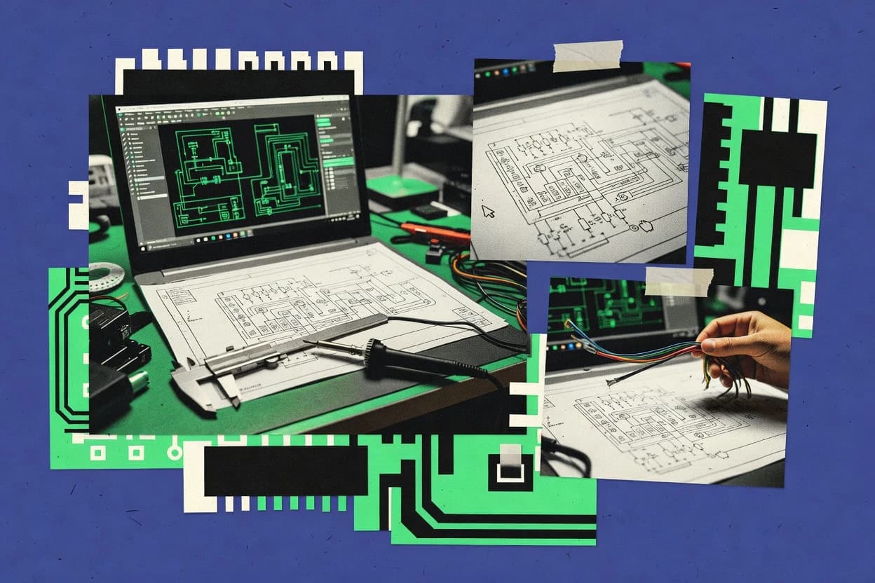
What Is Electronic Schematic Software?
Electronic schematic software is the CAD environment used to place components, draw nets, label signals, and generate netlists that connect schematics to PCB design. It solves wiring correctness problems by enforcing electrical rule checks like ERC on wiring and connectivity. It also solves manufacturing handoff problems by linking schematics to PCB footprints and by producing outputs such as Gerber files and drill and placement data in tools like Autodesk EAGLE. Examples of integrated workflows include Altium Designer for schematic-to-PCB connectivity synchronization and KiCad for hierarchical schematics with ERC-based integrity checks.
Key Features to Look For
Evaluation should focus on the exact schematic-to-layout integrity mechanisms and workflow depth that prevent connectivity mistakes and accelerate iteration in real projects.
Live schematic-to-PCB net connectivity synchronization
Live schematic-to-PCB connectivity prevents many mismatches by keeping schematic nets and PCB objects aligned through shared design data. Autodesk EAGLE stands out with a tight schematic-to-PCB link with live net connectivity, and Altium Designer delivers smart connectivity via synchronized schematic and PCB objects.
Electrical Rule Check and design rule feedback loops
ERC and DRC feedback loops catch connectivity and fabrication-rule violations early so errors do not reach routing or manufacturing stages. Autodesk EAGLE integrates ERC and DRC to catch connectivity and clearance and footprint mismatches, and KiCad includes hierarchical sheets with Electrical Rule Check integration.
Hierarchical multi-sheet schematic organization
Hierarchical sheets scale complex designs by structuring subsheets while keeping net connectivity traceable across the project. Autodesk EAGLE supports hierarchical multi-sheet projects, and KiCad provides hierarchical schematic sheets with clear connectivity across subsheets.
Robust library and footprint management for consistent symbols
Reliable symbol and footprint libraries reduce manual setup and help keep parts consistent across schematic edits and PCB layout. Autodesk EAGLE offers vast part and footprint libraries, KiCad includes symbol and footprint libraries with editors for customization, and EasyEDA links online component search to schematic symbols and PCB footprints.
Simulation capability driven from schematic design
Schematic-driven simulation helps validate logic, analog behavior, or microcontroller interactions before manufacturing. Proteus Design Suite pairs schematic capture with mixed-signal simulation and uses microcontroller co-simulation with virtual peripherals, while the reviewed desktop PCB-focused suites like KiCad and Autodesk EAGLE keep simulation as less unified compared with dedicated SPICE-focused workflows.
Manufacturing and downstream export outputs
Fabrication-ready outputs reduce handoff friction when schematic and PCB data must become board production files. Autodesk EAGLE outputs Gerber exports plus drill and placement files, while EasyEDA exports fabrication-ready PCB files directly from the PCB workspace.
How to Choose the Right Electronic Schematic Software
Selection should follow the target workflow first, then validate that the tool’s connectivity checks, library handling, and outputs match the project scale and verification needs.
Match the tool to the real end goal: schematic-only, schematic-to-PCB, or simulation-first
If the end goal is manufacturing-ready boards with tight schematic-to-layout integrity, Autodesk EAGLE and Altium Designer focus on integrated schematic-to-PCB connectivity and rule feedback. If the end goal includes verifying embedded circuits before layout completion, Proteus Design Suite runs mixed-signal simulation directly from the schematic and supports microcontroller co-simulation with virtual instruments and peripherals.
Prioritize connectivity integrity by checking how netlists stay synchronized
Connectivity should be managed through shared design data and synchronized schematic and PCB objects to reduce orphan pin and broken net issues. Altium Designer’s smart connectivity keeps schematic and PCB objects synchronized via shared design data, and Mentor Graphics PADS maintains connectivity synchronization through netlist transfer to PADS PCB with schematic changes propagating into board connectivity.
Scale with hierarchical design and project-level organization
Complex projects need hierarchical multi-sheet organization so nets remain traceable across subsheets and blocks. Autodesk EAGLE supports hierarchical multi-sheet schematics, and KiCad provides hierarchical sheets that integrate ERC checks to catch wiring and pin and netlabel issues early.
Use rules and constraint mechanisms that align with routing and fabrication risks
If fabrication rule compliance matters during schematic entry and routing, tools like Autodesk EAGLE with integrated ERC and DRC and OrCAD Capture plus Allegro with constraint-driven design checks reduce time spent on late-stage fixes. OrCAD Capture and Allegro enforce design checks from schematic connectivity inside Allegro PCB Editor, which helps keep dense boards aligned with routing and rule constraints.
Choose workflow speed and library workflow fit for the team’s operating style
Browser-based workflows benefit teams that want quick access and rapid part selection through online search, which is a strength of EasyEDA through online component search linked to schematic symbols and PCB footprints. Teams that need lightweight drawing and netlists for straightforward documentation can use TinyCAD for rapid symbol placement and wire routing, while engineers doing fast integrated board iteration can use DipTrace for rules-driven PCB checks with schematic-to-layout consistency enforcement.
Who Needs Electronic Schematic Software?
Electronic schematic software benefits teams and individuals who must create correct wiring, maintain consistent symbols and footprints, and transform schematics into PCB-ready connectivity and documentation.
Single-team electronics design needing reliable schematic-to-PCB handoff
Autodesk EAGLE is a strong fit because it integrates schematic capture with PCB layout in one workspace and keeps live net connectivity consistent as layouts evolve. Its ERC and DRC catch connectivity and fabrication rule issues early and its Gerber, drill, and placement exports streamline manufacturing handoff.
Large teams building mixed-signal and high-speed hardware with strong design rule control
Altium Designer fits team scale because its smart connectivity synchronizes schematic and PCB objects via shared design data and supports large designs through hierarchical sheets and reusable blocks. Its constraint-driven DRC gives immediate feedback on rule violations and it includes integrated signal integrity tooling to support verification for high-speed designs.
Open hardware teams that require schematic integrity checks and PCB-ready output
KiCad supports open hardware workflows using open-source integrated schematic capture and PCB design with ERC checks tailored to electrical rules. Its hierarchical sheets keep connectivity traceable across subsheets and its tight schematic-to-footprint linking supports consistent netlist export.
Teams validating embedded electronics with schematic-driven mixed-signal simulation
Proteus Design Suite matches the need for simulation before manufacturing because it runs mixed-signal simulation directly from the schematic design and supports microcontroller co-simulation. It also uses probe instruments and stimulus components for testbench-style validation tied to the schematic.
Common Mistakes to Avoid
Many projects fail later due to predictable mismatches between how schematics define intent and how the tool enforces connectivity, rules, and hierarchy as the design grows.
Choosing a tool without synchronized schematic-to-PCB connectivity
Connectivity mistakes rise when schematic nets do not remain synchronized with PCB objects during edits, which is the area where Autodesk EAGLE and Altium Designer are designed to keep net connectivity consistent. OrCAD Capture plus Allegro also reduces mismatches by enforcing Allegro PCB Editor design rule checks from schematic connectivity.
Ignoring ERC and DRC feedback during early wiring and routing
Late discovery of clearance and footprint mismatches creates costly rework, which Autodesk EAGLE mitigates with integrated ERC and DRC while Altium Designer mitigates with constraint-driven DRC feedback. KiCad’s ERC integration on hierarchical sheets helps catch wiring pin and netlabel issues early.
Underestimating how library management impacts real project iteration
Symbol and footprint inconsistency slows parts selection and increases rework, which Autodesk EAGLE addresses with vast part and footprint libraries and which KiCad addresses with symbol and footprint editors. EasyEDA accelerates part placement by linking online component search to schematic symbols and PCB footprints.
Expecting deep simulation from a PCB-focused schematic workflow
Tools focused on connectivity and fabrication outputs may not provide unified SPICE-like analysis, which is why Proteus Design Suite is positioned for mixed-signal and microcontroller simulation with virtual instruments. Autodesk EAGLE and KiCad keep simulation capabilities less unified than dedicated SPICE-focused workflows, so simulation-heavy verification should use Proteus Design Suite.
How We Selected and Ranked These Tools
We evaluated every tool on three sub-dimensions with features weighted at 0.4, ease of use weighted at 0.3, and value weighted at 0.3. The overall rating equals 0.40 × features plus 0.30 × ease of use plus 0.30 × value. Autodesk EAGLE separated from lower-ranked tools because its integrated schematic-to-layout workflow provides live net connectivity plus ERC and DRC feedback plus Gerber and drill and placement exports that streamline manufacturing handoff. This combination of features depth, workflow cohesion, and practical output support is reflected in the tool’s high overall score.
Frequently Asked Questions About Electronic Schematic Software
Which electronic schematic tools keep schematic-to-PCB connectivity synchronized with minimal manual rework?
What software best supports high-speed or mixed-signal projects where layout feedback must match schematic intent?
Which tools provide Electrical Rule Check features that catch schematic issues before layout begins?
Which option is strongest for mixed-signal validation using a schematic-driven simulation workflow?
Which tools are most suitable for open hardware workflows that prioritize portability and exportability?
What is the most common workflow for large multi-sheet projects across schematic and PCB stages?
Which browser-based option helps teams iterate quickly on schematic capture and PCB placement without local installation complexity?
Which tools focus on producing clean schematics and printable documentation with lightweight project management?
What toolchain best supports teams that need detailed manufacturing outputs and fabrication file generation from PCB designs?
Conclusion
After evaluating 10 manufacturing engineering, Autodesk EAGLE stands out as our overall top pick — it scored highest across our combined criteria of features, ease of use, and value, which is why it sits at #1 in the rankings above.
Use the comparison table and detailed reviews above to validate the fit against your own requirements before committing to a tool.
Tools reviewed
Primary sources checked during evaluation.
Referenced in the comparison table and product reviews above.
Keep exploring
Comparing two specific tools?
Software Alternatives
See head-to-head software comparisons with feature breakdowns, pricing, and our recommendation for each use case.
Explore software alternatives→In this category
Manufacturing Engineering alternatives
See side-by-side comparisons of manufacturing engineering tools and pick the right one for your stack.
Compare manufacturing engineering tools→FOR SOFTWARE VENDORS
Not on this list? Let’s fix that.
Our best-of pages are how many teams discover and compare tools in this space. If you think your product belongs in this lineup, we’d like to hear from you—we’ll walk you through fit and what an editorial entry looks like.
Apply for a ListingWHAT THIS INCLUDES
Where buyers compare
Readers come to these pages to shortlist software—your product shows up in that moment, not in a random sidebar.
Editorial write-up
We describe your product in our own words and check the facts before anything goes live.
On-page brand presence
You appear in the roundup the same way as other tools we cover: name, positioning, and a clear next step for readers who want to learn more.
Kept up to date
We refresh lists on a regular rhythm so the category page stays useful as products and pricing change.