GITNUXSOFTWARE ADVICE
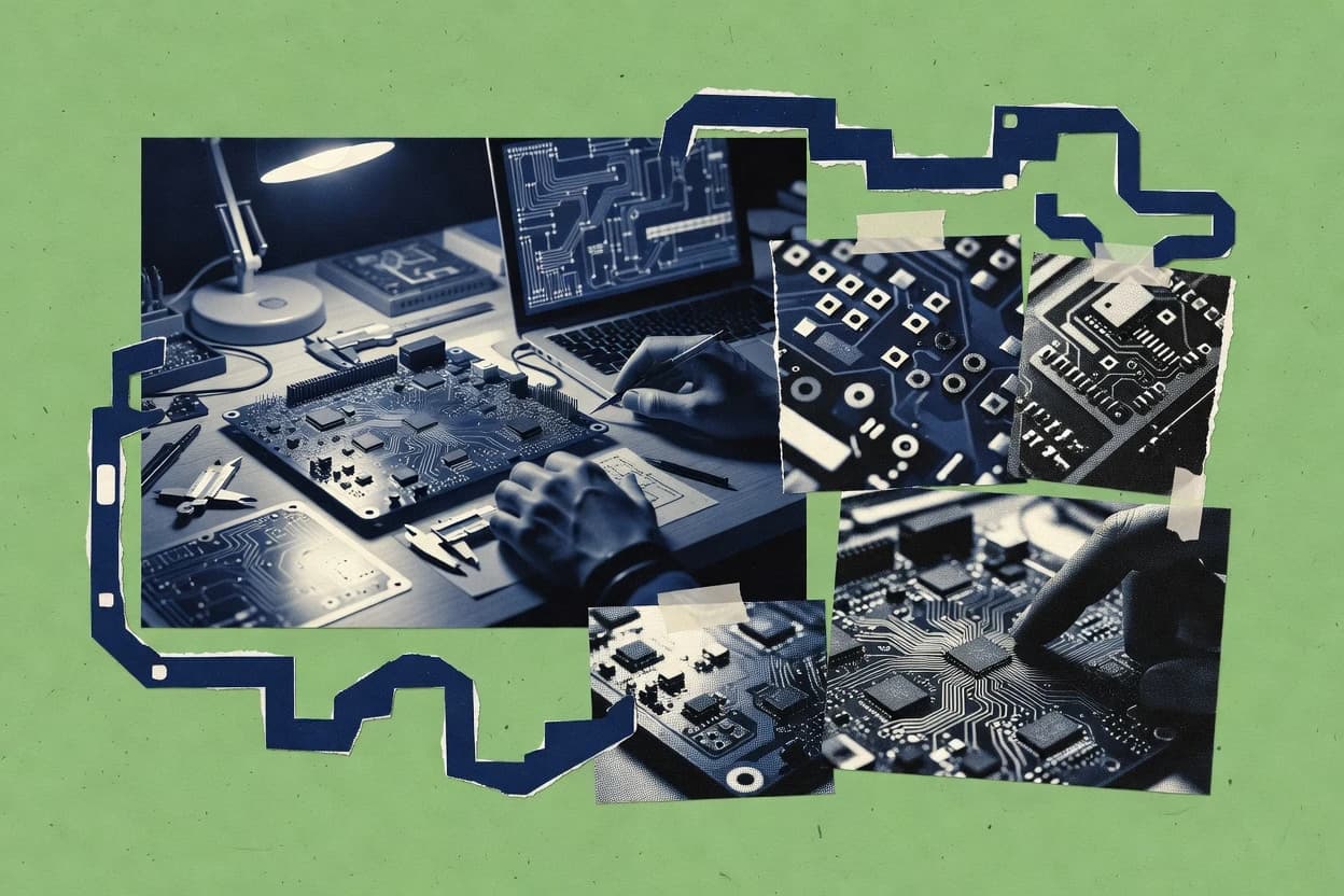
Manufacturing EngineeringTop 10 Best Electronic Pcb Design Software of 2026
Top 10 Electronic Pcb Design Software ranking with Autodesk EAGLE, Altium Designer, KiCad and more. Compare tools and pick the best.

How we ranked these tools
Core product claims cross-referenced against official documentation, changelogs, and independent technical reviews.
Analyzed video reviews and hundreds of written evaluations to capture real-world user experiences with each tool.
AI persona simulations modeled how different user types would experience each tool across common use cases and workflows.
Final rankings reviewed and approved by our editorial team with authority to override AI-generated scores based on domain expertise.
Score: Features 40% · Ease 30% · Value 30%
Gitnux may earn a commission through links on this page — this does not influence rankings. Editorial policy
Editor’s top 3 picks
Three quick recommendations before you dive into the full comparison below — each one leads on a different dimension.
Autodesk EAGLE
Design-rule checking with netclasses and constraint-based enforcement during layout
Built for indie teams needing efficient PCB layout with reliable DRC and fabrication outputs.
Altium Designer
Editor pickIntegrated Constraint Manager enforces electrical and design rules across schematic and PCB
Built for large electronics teams needing constraint-driven PCB design and strong CAM outputs.
KiCad
Editor pickUnified netlist-driven workflow across schematic, layout, and rule-based checks
Built for engineers needing complete schematic-to-layout PCB design with deterministic exports.
Related reading
Comparison Table
This comparison table benchmarks Electronic PCB design software across feature sets, design workflows, and file compatibility for tools such as Autodesk EAGLE, Altium Designer, KiCad, CADSTAR, and OrCAD Capture with OrCAD PCB Designer. The entries highlight differences in schematic capture, PCB layout capabilities, library and component management, and typical project handoff paths so readers can map tool choice to their production requirements.
Autodesk EAGLE
electronics EDAEDA workflows for schematic capture, PCB layout, and manufacturing-ready outputs inside the Autodesk environment.
Design-rule checking with netclasses and constraint-based enforcement during layout
Autodesk EAGLE stands out for its fast schematic-to-layout workflow and tight library management in a single editor suite. It supports schematic capture, PCB layout with interactive routing, and design-rule checking for manufacturability checks before export.
The tool integrates component packaging and symbol libraries, plus pattern-based placement tools that speed board assembly from existing designs. Export options cover common fabrication outputs like Gerber and drill files, which streamlines handoff to PCB manufacturers.
- +Integrated schematic capture and PCB layout in one workflow.
- +Interactive autorouting with manual override for precise control.
- +Design-rule checking catches clearances and routing constraint issues.
- +Library-driven components with consistent symbols and footprints.
- +Gerber and drill exports for direct fabrication handoff.
- +Batch updates help keep footprints and footprints variants aligned.
- –Less suited for large multi-sheet projects than higher-end systems.
- –Routing can feel slower on dense boards than modern CAD engines.
- –Advanced simulation workflows require separate tools and setup.
- –Version control is not deeply integrated for collaborative teams.
- –Customization relies heavily on scripting conventions and templates.
Best for: Indie teams needing efficient PCB layout with reliable DRC and fabrication outputs
More related reading
Altium Designer
advanced PCBPCB design with schematic-to-layout integration, advanced routing, and electronics manufacturing output generation.
Integrated Constraint Manager enforces electrical and design rules across schematic and PCB
Altium Designer stands out for its tightly integrated schematic-to-PCB workflow that uses the same design data across tools. The platform supports rule-driven PCB design with interactive constraints, 3D PCB visualization, and robust fabrication outputs via native CAM capabilities.
It also includes advanced library management for components, footprints, and parametric models to reduce layout rework. For complex boards, it provides signal integrity and simulation-driven validation paths alongside standard electronics design features.
- +Schematic and PCB stay synchronized with shared design database
- +Rule-driven design helps prevent constraint violations during routing
- +Interactive 3D visualization supports mechanical and placement review
- +Native CAM output accelerates fabrication data generation
- +Powerful component and footprint library management reduces duplication
- –High feature depth increases setup and workflow learning time
- –Resource usage can spike on large multi-layer projects
- –Some automation requires careful rules configuration to behave correctly
- –UI density can slow navigation for new users
Best for: Large electronics teams needing constraint-driven PCB design and strong CAM outputs
KiCad
open-source EDAOpen-source schematic capture and PCB layout with libraries and design rule checks for production files.
Unified netlist-driven workflow across schematic, layout, and rule-based checks
KiCad stands out for combining schematic capture and PCB layout in a single open-source workflow with shared libraries. It supports net connectivity, ERC and DRC checks, and PCB rule configuration for controlled manufacturing outputs.
The tool generates manufacturing files like Gerbers, drill data, and 3D visualizations to validate builds before export. KiCad also includes symbol and footprint management that helps teams standardize components across projects.
- +Tight schematic-to-PCB connectivity with consistent netlist-driven placement
- +Robust DRC and ERC rules for catching electrical and layout issues early
- +Generates Gerbers, drill files, and position files for fabrication workflows
- +Active library ecosystem with symbols and footprints for many common parts
- –Complex rule configuration can feel technical for new users
- –Large boards may require careful performance tuning on typical hardware
- –3D visualization depends on accurate footprints and model setup
- –Custom workflows often require manual tooling between steps
Best for: Engineers needing complete schematic-to-layout PCB design with deterministic exports
CADSTAR
industrial PCBProfessional PCB design tooling for industrial electronics engineering teams that need robust layout and DFM outputs.
Constraint-driven DRC tied directly to schematic-to-PCB connectivity within the same design database
CADSTAR by mentor.com stands out with a tight schematic-to-PCB workflow built around Mentor design data management conventions. The suite supports schematic capture, interactive PCB layout, constraint-driven design checks, and fabrication output generation from a unified design database.
CADSTAR includes library handling for symbols and footprints, plus connectivity validation to reduce routing and DRC rework across revisions. It is positioned for electronics teams that need consistent design rules and repeatable production exports for multi-board projects.
- +Schematic to PCB connectivity checks reduce routing mistakes
- +Constraint-driven design rules support controlled high-integrity layouts
- +Accurate fabrication and documentation outputs from the same design data
- +Library management streamlines reuse of symbols and footprints
- –Workflow can feel process-heavy for quick one-off boards
- –Advanced routing and rule editing require careful setup
- –Learning curve is steep for teams moving from simpler editors
Best for: Teams needing controlled PCB design rules with repeatable production outputs
OrCAD Capture and OrCAD PCB Designer
schematic-to-PCBSchematic entry and PCB layout capabilities that support production data generation for manufacturing engineering.
Schematic-driven netlist transfer into OrCAD PCB Designer with connectivity validation
OrCAD Capture combines schematic entry with rules-aware design checks and exports to OrCAD PCB Designer workflows. OrCAD PCB Designer supports interactive PCB layout with constraint-driven placement, route optimization, and robust library-driven component management.
Tool links between schematic and PCB reduce rework by propagating net connectivity and design intent across the capture-to-layout flow. This package targets full PCB design deliverables including documentation, electrical connectivity validation, and production-ready layout preparation.
- +Tight schematic-to-PCB link preserves net connectivity and design intent
- +Constraint-driven routing improves consistency for larger PCB layouts
- +Rule checks catch electrical and connectivity issues before release
- +Library-based component management speeds reuse across projects
- –Editing large schematics can feel slower than modern UI layouts
- –Advanced DRC tuning requires careful setup to avoid noisy results
- –Complex stackup and impedance workflows demand experienced parameter management
Best for: Teams producing conventional PCB designs with rule checks and strong schematic-to-layout traceability
Proteus Design Suite
simulation-firstEDA plus mixed-mode simulation workflows that include schematic capture and PCB layout for hardware verification.
Mixed-signal simulation using virtual instruments directly within the Proteus design workflow
Proteus Design Suite pairs schematic capture, PCB layout, and deep mixed-signal simulation in one workflow. Components can be wired in virtual hardware and validated with instrument models such as oscilloscopes and logic analyzers.
PCB routing supports standard copper features like tracks, vias, polygons, and design-rule checking tied to the layout. Library-driven component management links simulation symbols to physical PCB footprints for board-level verification.
- +Mixed-signal simulation with instrument models like scopes and logic analyzers
- +Schematic to PCB workflow with linked symbols and footprints
- +Design-rule checking catches PCB rule violations during routing
- +Integrated library management supports reusable component definitions
- –Advanced simulation setup can feel technical for complex projects
- –Large PCB layouts require careful workflow management to stay responsive
- –Footprint correctness depends heavily on library and mapping quality
Best for: Engineers validating designs with simulation instruments and then producing PCB layouts
Zuken CR-8000
enterprise PCBPCB design platform for large-scale electronics engineering with data management and manufacturing-ready deliverables.
Schematic-to-PCB connectivity management with configurable design-rule enforcement
Zuken CR-8000 stands out with integrated electronic design workflows that connect schematic capture to PCB layout with strong routing control. It supports rules-driven design using configurable constraints for nets, components, and manufacturing requirements.
The tool focuses on engineering data reuse and design consistency across revisions through project management features and verification workflows. It is particularly geared toward structured board development where connectivity accuracy and layout compliance checks are central to delivery.
- +Rules-driven design checks catch constraint violations during layout and editing
- +Tight schematic-to-layout connectivity reduces netlist sync errors
- +Interactive routing options support controlled high-quality board traces
- +Verification workflows help validate connectivity and design rule compliance
- +Structured project data helps manage changes across design revisions
- –Complex configuration can slow initial setup for custom design rules
- –Advanced routing workflows require experienced layout practices
- –UI and command flows can feel heavy for small board projects
- –Integration depth can add overhead when designs change frequently
- –Reporting and handoff formats may require extra configuration
Best for: Teams needing rules-driven PCB design consistency across structured revisions
Target 3001!
budget PCBPCB layout and autorouting software that supports schematic-to-PCB creation and export to fabrication formats.
Built-in design-rule checking with layer-aware routing and constraint enforcement
Target 3001! from Elektor focuses on circuit-board design with a workflow built around practical PCB drafting and routing. It supports schematic-driven and freehand PCB layouts, with tools for component placement, track routing, and design-rule checking.
The package includes board manufacturing outputs such as drill and layer plots and integrates common footprint and library management for component reuse. It is especially suited to engineers producing single boards and small runs who want tight control over layout details and export readiness.
- +Strong PCB layout and track routing with fast interactive editing
- +Design-rule checking helps catch spacing and clearance violations early
- +Manufacturing output generation covers drill and fabrication layer exports
- +Footprint and library handling supports repeatable component placement
- –Schematic integration can feel less streamlined than dedicated ECAD suites
- –Advanced signal-integrity style analysis is limited
- –Large, complex projects can be slower to navigate and edit
- –3D visualization depth for enclosure-fit checks is not comprehensive
Best for: Engineers designing single PCBs needing detailed layout control and reliable exports
EasyEDA
cloud EDABrowser-based schematic capture and PCB layout with fabrication-file generation for electronics manufacturing.
Integrated Gerbers and drill export directly from web-based schematic-to-PCB projects
EasyEDA stands out for running an integrated electronic design workflow in a web editor that supports schematic, PCB layout, and simulation access in one environment. Core capabilities include symbol and footprint libraries, schematic capture, rule-based PCB routing, and interactive 3D preview of the board model.
The tool also supports design verification through DRC and net checks tied to the schematic connectivity. Export options cover manufacturing outputs like Gerbers and drill files to support fabrication handoff.
- +Web-based schematic and PCB layout in one continuous workspace
- +DRC and net connectivity checks reduce layout-to-schematic mismatches
- +Integrated 3D board preview helps validate component placement and clearances
- +Library search supports quick reuse of parts and footprints
- +Manufacturing export outputs Gerbers and drill files from one project
- –Advanced routing control can feel less granular than desktop CAD suites
- –Complex multi-sheet designs may require careful management of sheet hierarchy
- –Simulation workflows are limited compared with dedicated EDA simulators
- –Constraint-driven workflows rely on setting rules correctly upfront
Best for: Teams needing browser-based PCB design with manufacturing-ready output generation
CircuitMaker
PCB designPCB design tool with schematic capture and layout aimed at maker-to-professional electronics production workflows.
Auto net linking from schematic capture to PCB layout
CircuitMaker centers on a free-form PCB editor paired with an integrated component and footprint workflow designed for practical board layout. It supports schematic capture, library-driven symbol and footprint placement, and detailed PCB routing with clear constraint handling for traces, nets, and layers.
The CAM and Gerber export pipeline supports manufacturing handoff with common PCB data outputs. It also includes design rule checking to catch clearance, connectivity, and basic manufacturing errors before exporting.
- +Schematic-to-PCB flow links nets automatically for faster layout setup
- +Solid routing tools with multi-layer support and controllable trace behavior
- +Design rule checking flags clearance and connectivity issues early
- +Library workflow helps standardize symbols and footprints across projects
- +Gerber and CAM outputs support straightforward fabrication handoff
- –Less comprehensive advanced simulation compared with dedicated EDA simulators
- –Footprint management can feel rigid for heavily customized parts
- –Component placement and floorplanning features are simpler than premium suites
Best for: Hobbyists and small teams making manufacturable PCB layouts from schematics
How to Choose the Right Electronic Pcb Design Software
This buyer’s guide covers how to select electronic PCB design software across tools including Autodesk EAGLE, Altium Designer, KiCad, CADSTAR, OrCAD Capture and OrCAD PCB Designer, Proteus Design Suite, Zuken CR-8000, Target 3001!, EasyEDA, and CircuitMaker. It maps concrete design workflows like schematic-to-PCB synchronization, constraint-driven routing, and fabrication output generation to the actual strengths and tradeoffs those tools deliver.
What Is Electronic Pcb Design Software?
Electronic PCB design software is used to create schematic capture, translate net connectivity into PCB layout, route tracks and vias, and run design-rule checks that verify electrical and manufacturing constraints. These tools generate fabrication-ready outputs such as Gerbers and drill files so manufacturing teams can build the board from the same design intent. Autodesk EAGLE demonstrates a schematic-to-layout workflow with design-rule checking using netclasses and constraint enforcement before export. KiCad demonstrates an open-source schematic-to-PCB flow with unified netlist-driven connectivity plus ERC and DRC rule checks that produce Gerbers and drill data.
Key Features to Look For
These features determine whether a PCB design stays consistent from schematic intent to manufacturable layout without creating rework.
Unified schematic-to-PCB connectivity
Unified schematic-to-PCB connectivity prevents netlist drift and routing mistakes by keeping schematic intent and PCB connectivity linked. KiCad excels with a unified netlist-driven workflow across schematic, layout, and rule-based checks, and OrCAD Capture with OrCAD PCB Designer links between schematic entry and PCB designer workflows using connectivity validation.
Constraint-driven design-rule checking
Constraint-driven DRC and rule-based enforcement catches clearance, connectivity, and routing constraint violations while layout is still being created. Altium Designer provides an integrated Constraint Manager that enforces electrical and design rules across schematic and PCB, and CADSTAR ties constraint-driven DRC directly to schematic-to-PCB connectivity within the same design database.
Manufacturing output generation for fabrication handoff
Reliable fabrication outputs reduce downstream errors by producing the exact documentation that board houses request. Autodesk EAGLE exports common fabrication outputs like Gerber and drill files, and EasyEDA generates Gerbers and drill files directly from web-based schematic-to-PCB projects.
Interactive routing with manual override
Interactive routing with controllable autorouting speeds board completion while still enabling precise constraint control on dense sections. Autodesk EAGLE supports interactive autorouting with manual override, and CircuitMaker provides solid routing tools with controllable trace behavior plus multi-layer routing.
Library management for symbols and footprints
Strong library management reduces rework by ensuring schematic components map to correct PCB footprints and 3D models. Autodesk EAGLE uses library-driven components with consistent symbols and footprints and supports batch updates for keeping footprints aligned, while Altium Designer emphasizes advanced library management for components, footprints, and parametric models.
3D visualization tied to placement and clearances
3D visualization supports enclosure-fit and mechanical review using the PCB model and component placement. Altium Designer includes interactive 3D PCB visualization for mechanical and placement review, and EasyEDA provides an integrated 3D board preview to validate component placement and clearances.
How to Choose the Right Electronic Pcb Design Software
The right choice depends on whether the workflow must be constraint-driven, schematic-to-PCB-synchronized, simulation-integrated, or output-focused for quick fabrication handoff.
Match the workflow to the level of schematic-to-layout synchronization needed
If schematic and PCB must stay synchronized through netlist-driven connectivity checks, choose KiCad or CADSTAR where connectivity and rule verification are built around the same design database concepts. If production traceability from capture to layout is essential, choose OrCAD Capture with OrCAD PCB Designer because netlist transfer into the PCB designer includes connectivity validation.
Prioritize constraint enforcement when the board must meet controlled electrical and manufacturing rules
For designs that require rule-driven layout to prevent constraint violations during routing, Altium Designer and CADSTAR are direct fits because they enforce electrical and design rules with integrated constraint mechanisms. Autodesk EAGLE also supports design-rule checking using netclasses and constraint-based enforcement during layout, which reduces manual clearance and routing mistakes before export.
Select the fabrication handoff model that fits the deliverables expected by manufacturing
If Gerber and drill outputs need to come straight from the same project used to do layout, Autodesk EAGLE and EasyEDA are strong picks because both generate Gerbers and drill files as core outputs. If a workflow must include board-level documentation and production-ready layout preparation, OrCAD Capture and OrCAD PCB Designer targets production deliverables with rule checks and exports aligned to the capture-to-layout flow.
Decide whether simulation-in-loop is a requirement or a separate toolchain
If mixed-signal verification must happen inside the same environment where PCB routing is performed, Proteus Design Suite supports mixed-signal simulation using virtual instruments like oscilloscopes and logic analyzers plus linked PCB layout validation. If simulation is not required inside the editor, Autodesk EAGLE stays focused on schematic capture, interactive routing, DRC, and manufacturing outputs.
Pick the tool whose editing depth matches board size and complexity
For large multi-layer boards where constraint handling and CAM workflows matter, Altium Designer is a fit because resource usage increases on large projects but the platform adds integrated CAM output generation. For single boards and small runs where detailed layout control and fast interactive editing matter, Target 3001! supports layer-aware routing with built-in design-rule checking plus drill and fabrication layer exports.
Who Needs Electronic Pcb Design Software?
Electronic PCB design software benefits teams and engineers who must translate schematic connectivity into manufacturable physical layouts with rules checks and fabrication-ready exports.
Indie teams that need an efficient schematic-to-layout path with DRC and fabrication outputs
Autodesk EAGLE fits because it delivers integrated schematic capture and PCB layout in one workflow plus design-rule checking with netclasses and constraint-based enforcement before Gerber and drill export. CircuitMaker also fits for practical layout completion because it links nets automatically from schematic capture and provides Gerber and CAM outputs with DRC flags for clearance and connectivity.
Large electronics teams that must manage complex constraints and generate fabrication data efficiently
Altium Designer is designed for large electronics teams needing rule-driven PCB design with constraint management and native CAM output generation. CADSTAR fits teams that need repeatable production exports across multi-board projects with constraint-driven DRC tied directly to schematic-to-PCB connectivity within a unified design database.
Engineers who want deterministic open-source schematic-to-PCB exports with ERC and DRC
KiCad is positioned for engineers needing a complete schematic-to-layout PCB design workflow with ERC and DRC plus unified netlist-driven rule checks. Target 3001! fits engineers focusing on detailed single-board routing with built-in design-rule checking and manufacturing outputs like drill and layer plots.
Engineers who must validate designs using instrument-driven mixed-signal simulation while building PCB layout
Proteus Design Suite fits because it pairs schematic capture, PCB layout, and mixed-signal simulation with virtual instruments such as oscilloscopes and logic analyzers. Zuken CR-8000 fits teams building structured revisions that depend on schematic-to-PCB connectivity management and configurable design-rule enforcement.
Common Mistakes to Avoid
Several recurring pitfalls appear across these tools when projects push beyond the intended workflow model.
Choosing a tool without built-in constraint enforcement for rule-critical boards
Altium Designer supports an integrated Constraint Manager that enforces electrical and design rules across schematic and PCB, which reduces routing-time violations. CADSTAR ties constraint-driven DRC directly to schematic-to-PCB connectivity within the same design database, which helps prevent rule gaps during revision changes.
Letting schematic-to-PCB connectivity drift before layout is finalized
KiCad provides a unified netlist-driven workflow so schematic connectivity maps deterministically into layout and rule-based checks. OrCAD Capture with OrCAD PCB Designer also reduces rework by propagating net connectivity and design intent into the PCB designer with connectivity validation.
Underestimating setup complexity for advanced rule configuration
KiCad and Zuken CR-8000 both involve complex rule configuration that can feel technical for new users, which slows early productivity without a clear rule strategy. CADSTAR and Altium Designer also require careful rule setup so automation behaves correctly and DRC tuning avoids noisy results.
Assuming advanced simulation and board verification exist in the same workflow
Proteus Design Suite is built to include mixed-signal simulation with virtual instruments inside the same design workflow. Autodesk EAGLE can require separate tools for advanced simulation workflows, so simulation expectations should align with the chosen toolchain.
How We Selected and Ranked These Tools
we evaluated every tool on three sub-dimensions: features with weight 0.4, ease of use with weight 0.3, and value with weight 0.3. The overall rating is the weighted average of those three dimensions using overall = 0.40 × features + 0.30 × ease of use + 0.30 × value. Autodesk EAGLE separated from lower-ranked tools by combining a high feature score with high ease of use through integrated schematic capture and PCB layout plus interactive autorouting and DRC tied to netclasses. Autodesk EAGLE also strengthened the overall result by delivering fabrication exports like Gerber and drill files from the same workflow that performs the layout checks.
Frequently Asked Questions About Electronic Pcb Design Software
Which electronic PCB design software gives the most reliable schematic-to-layout handoff?
How do Altium Designer, Autodesk EAGLE, and KiCad differ in their approach to design-rule checking?
Which tool is best suited for teams that need strong CAM-style fabrication outputs from the same workspace?
What software supports mixed-signal simulation tied to PCB layout rather than simulation as a separate step?
Which options are strongest for managing complex libraries and parametric component definitions?
Which tools best support interactive routing control with constraint-driven placement?
Which software fits multi-board engineering projects where design data reuse and revision consistency matter?
Which tool is best for browser-based PCB design work with built-in manufacturing output generation?
What should be used when starting from a drafted PCB approach or needing freehand layout control?
Which software is a strong choice for validating connectivity and manufacturability issues before exporting files?
Conclusion
After evaluating 10 manufacturing engineering, Autodesk EAGLE stands out as our overall top pick — it scored highest across our combined criteria of features, ease of use, and value, which is why it sits at #1 in the rankings above.
Use the comparison table and detailed reviews above to validate the fit against your own requirements before committing to a tool.
Tools reviewed
Primary sources checked during evaluation.
Referenced in the comparison table and product reviews above.
Keep exploring
Comparing two specific tools?
Software Alternatives
See head-to-head software comparisons with feature breakdowns, pricing, and our recommendation for each use case.
Explore software alternatives→In this category
Manufacturing Engineering alternatives
See side-by-side comparisons of manufacturing engineering tools and pick the right one for your stack.
Compare manufacturing engineering tools→FOR SOFTWARE VENDORS
Not on this list? Let’s fix that.
Our best-of pages are how many teams discover and compare tools in this space. If you think your product belongs in this lineup, we’d like to hear from you—we’ll walk you through fit and what an editorial entry looks like.
Apply for a ListingWHAT THIS INCLUDES
Where buyers compare
Readers come to these pages to shortlist software—your product shows up in that moment, not in a random sidebar.
Editorial write-up
We describe your product in our own words and check the facts before anything goes live.
On-page brand presence
You appear in the roundup the same way as other tools we cover: name, positioning, and a clear next step for readers who want to learn more.
Kept up to date
We refresh lists on a regular rhythm so the category page stays useful as products and pricing change.