GITNUXSOFTWARE ADVICE
Manufacturing EngineeringTop 8 Best Ic Package Design Software of 2026
Top 10 Ic Package Design Software tools ranked for PCB design, DRC checks, and routing. Compare picks like Cadence Allegro and Altium.

How we ranked these tools
Core product claims cross-referenced against official documentation, changelogs, and independent technical reviews.
Analyzed video reviews and hundreds of written evaluations to capture real-world user experiences with each tool.
AI persona simulations modeled how different user types would experience each tool across common use cases and workflows.
Final rankings reviewed and approved by our editorial team with authority to override AI-generated scores based on domain expertise.
Score: Features 40% · Ease 30% · Value 30%
Gitnux may earn a commission through links on this page — this does not influence rankings. Editorial policy
Editor’s top 3 picks
Three quick recommendations before you dive into the full comparison below — each one leads on a different dimension.
Cadence Allegro Package Designer
IC package footprint creation with pin mapping and database-managed library consistency
Built for teams producing many IC footprints with strict library and verification needs.
Altium Designer
Editor pickIntegrated 3D-aware footprint and component library workflows within the Altium design environment
Built for teams designing IC package footprints with integrated PCB constraints and 3D.
Siemens PADS Professional
Editor pickRule-driven footprint and courtyard verification for IC package land patterns
Built for manufacturing-focused teams standardizing IC package footprints for PCB layout.
Related reading
Comparison Table
This comparison table reviews Ic package design software tools used for schematic-to-layout workflows, footprint creation, and constraint-driven placement for high-density assemblies. It groups leading solutions such as Cadence Allegro Package Designer, Altium Designer, Siemens PADS Professional, Mentor Graphics xDX Designer, and Ansys Electronics Desktop so readers can compare coverage across library management, routing and verification capabilities, and integration paths into simulation and manufacturing handoff. The table highlights the functional differences that impact package design throughput, design rule enforcement, and DFM-ready output.
Cadence Allegro Package Designer
EDA layoutAutomates and validates IC and package-related PCB footprints, escape routing, and package design flows with constraint-driven design and manufacturing-ready outputs.
IC package footprint creation with pin mapping and database-managed library consistency
Cadence Allegro Package Designer stands out for tight integration with Allegro PCB design workflows and library-driven package creation. It supports defining component package geometries, pin maps, and electrical and mechanical attributes used for downstream placement and manufacturing deliverables.
The tool focuses on accurate IC package footprint design, routing constraints, and visualization of pads, leads, and keepouts within package databases. It is designed for teams that require consistent reuse of package data and reliable handoff to PCB layout and verification flows.
- +Deep Allegro PCB integration for fast, reliable footprint-to-layout handoff
- +Strong package library management with reusable symbols and footprints
- +Accurate pad, lead, and keepout definition for manufacturable package footprints
- +Attribute and pin mapping supports consistent design data transfer
- –Footprint creation can feel heavy for small one-off package tweaks
- –Tooling requires disciplined library standards to avoid data drift
- –Learning curve is steep for advanced parameter and attribute workflows
Best for: Teams producing many IC footprints with strict library and verification needs
More related reading
Altium Designer
PCB/package designProvides footprint-driven PCB and package interconnect layout with advanced library management and fabrication and assembly export workflows.
Integrated 3D-aware footprint and component library workflows within the Altium design environment
Altium Designer stands out for its tight integration between schematic, PCB layout, and part footprint definition. It supports full IC package design workflows with 2D and 3D modeling tools and component library management for repeatable reuse.
Footprint generation workflows can be driven from component parameters, which helps standardize pin mapping and land patterns across packages. The environment also supports signal integrity oriented modeling through coordinated constraints from the PCB side into the package context.
- +Unified schematic-to-footprint-to-3D workflow in one toolchain
- +Parameter-driven footprint creation for consistent IC pin and land patterns
- +3D package visualization with accurate body and courtyard placement
- +Library structures support controlled reuse across large projects
- +Land pattern tooling aligns with PCB design rule checking
- –IC package editing can feel heavyweight for simple symbol updates
- –Deep setup of library automation requires training and careful organization
- –Managing large 3D asset sets increases project content complexity
- –Some package-specific utilities are less streamlined than dedicated library tools
Best for: Teams designing IC package footprints with integrated PCB constraints and 3D
Siemens PADS Professional
PCB/package designSupports constraint-based PCB and package footprint design with standard manufacturing data export for routing and assembly integration.
Rule-driven footprint and courtyard verification for IC package land patterns
Siemens PADS Professional stands out for its long-used PCB design workflows that integrate well with Siemens EDA tooling for industrial production needs. Ic Package Design focuses on defining package outlines and land patterns, then validating manufacturability through rule-driven checks and constraint management.
The environment supports mechanical integration steps, including courtyard and assembly considerations, alongside standard PCB capture-to-layout execution. Design reuse and library-driven component handling help teams maintain consistent IC package footprints across projects.
- +Rule-based validation catches package footprint and placement issues early
- +Library and reuse workflows reduce IC package footprint inconsistency risk
- +Supports mechanical integration with courtyard and assembly-oriented constraints
- +Stable PCB-centric flow aligns IC packages to physical assembly outputs
- –Complex rules and constraints can slow setup for new package types
- –Package-centric workflows still depend on external library curation
- –UI is oriented toward PCB layout, not package modeling depth
- –Advanced scripting automation requires additional skill and process overhead
Best for: Manufacturing-focused teams standardizing IC package footprints for PCB layout
Mentor Graphics xDX Designer
component integrationCreates and manages electronic design data for IC packaging and interconnects with structured components and layout constraints.
Rules-based constraint propagation across package geometry and manufacturing-relevant layouts
Mentor Graphics xDX Designer focuses on automated, model-driven integrated circuit package design workflows for high-density devices. It supports rules-based configuration and layout reuse through design templates and constraint management.
The tool integrates analysis-ready structures so package geometry changes propagate consistently across related views. It is commonly used to accelerate land pattern planning and manufacturing-driven documentation for IC packaging teams.
- +Model-driven workflow keeps package geometry and constraints consistently synchronized
- +Rule and template reuse speeds creation of variant package configurations
- +Constraint management improves design consistency across land pattern and mechanical elements
- –Template-driven setup can slow down highly bespoke packaging workflows
- –Complex constraints require careful upfront definition to avoid rework
- –Integration with nonstandard downstream formats can require manual adjustments
Best for: Packaging teams needing consistent, template-based IC package design automation
Ansys Electronics Desktop
EM simulationRuns electromagnetic and signal-integrity simulations for IC package interconnects and transitions to verify performance before manufacturing.
Electromagnetic modeling with S-parameter extraction for package-level interconnect analysis
Ansys Electronics Desktop stands out for combining full-wave electromagnetic simulation with IC package and interconnect modeling inside one analysis environment. It supports 3D EM workflows for leadframes, substrates, and bump or solder interconnects, with model setup tailored to package geometries.
It also integrates circuit co-simulation paths using S-parameter generation and data exchange, linking EM results to system-level signal integrity analysis. The toolset is driven by reusable geometry, meshing, and boundary-condition controls that help teams iterate package designs quickly.
- +Full-wave 3D EM modeling for IC packages and interconnects
- +S-parameter outputs ready for signal integrity and system co-simulation
- +Strong support for complex geometries like bumps, solder, and substrates
- +Workflow integration across EM, circuit, and system analysis
- –Setup complexity rises for large multi-die package assemblies
- –High-fidelity simulations can demand significant compute and memory
- –Learning curve is steep for boundary conditions and meshing strategy
Best for: Teams doing high-accuracy EM-driven IC package and interconnect design
COMSOL Multiphysics
multiphysicsSimulates thermo-mechanical and multiphysics effects in IC packages to assess stress, deformation, and thermal distribution.
Multiphysics coupling of electromagnetics with heat transfer and structural mechanics in one solve
COMSOL Multiphysics stands out with a tightly coupled multiphysics solver stack that connects electromagnetic fields, thermal behavior, and mechanical deformation in one simulation workflow. For IC package design, it supports 3D geometry import and meshing, material property definition, and boundary condition modeling for solder joints, substrates, and interconnect structures.
The platform enables parametric sweeps and optimization studies to evaluate effects like thermal gradients and strain on electrical performance. Results can be visualized with field plots, derived metrics, and scripted reports for repeatable design iterations.
- +Single environment for coupled EM, thermal, and structural simulations
- +Parametric sweeps and optimization studies for package design tradeoffs
- +High-fidelity 3D meshing with physics-specific element controls
- +Scriptable workflows for repeatable studies and custom post-processing
- –Complex setup requires careful physics and boundary condition selection
- –Large 3D coupled models can demand significant computational resources
- –Geometry repair and meshing cleanup can be time-intensive for imported CAD
- –Model management across many design variants can become cumbersome
Best for: Teams analyzing coupled thermal, structural, and EM impacts in IC packages
KiCad
open-source layoutDesigns PCB footprints and interconnect routing with an open workflow that supports manufacturing outputs for package-related boards.
Footprint editor with pad stack control and 3D STEP model association
KiCad stands out as a free, open-source EDA suite with a full schematic-to-PCB workflow and strong library support. It supports IC package design through footprint creation, courtyard and fab layer management, and 3D model linking via STEP for visualization.
Users can generate fabrication outputs like Gerbers and drill files from a single project while maintaining parametric footprint data. Design rule checking and netlist-driven updates help keep symbol pin mapping aligned with PCB pad geometry.
- +Schematic-to-PCB flow keeps pin mapping consistent through netlists
- +Footprint editor supports pad shapes, drill sizes, and layer assignments
- +3D viewer renders STEP models for mechanical fit checks
- –Advanced IC package automation needs manual footprint scripting
- –3D model handling depends on correct STEP scaling and origins
- –Large projects can feel slower during footprint and library edits
Best for: Teams designing custom IC footprints with repeatable fabrication outputs
Autodesk Fusion 360
3D mechanical CADProvides parametric 3D CAD for IC package modeling and assembly drawings used to generate step-based mechanical package definitions.
Parametric CAD design with linked assemblies and electronics documentation exports
Autodesk Fusion 360 stands out for unifying parametric CAD modeling with electronics-aware workflows inside one environment. It supports PCB and component-centric design through schematic-driven electronics documentation and 3D part modeling that links to manufacturing outputs.
For IC packaging work, it enables detailed geometry creation with constraints, assemblies, and tooling-ready exports. Its simulation and validation toolchain helps verify fit, motion, and thermal or structural behavior around the package.
- +Parametric modeling for repeatable IC package and footprint geometry changes
- +Associative electronics workflows tie modeled parts to documentation outputs
- +3D assembly constraints help validate lead, bump, and housing clearances
- –Packaging-specific libraries are limited compared with dedicated IC tools
- –Large package assemblies can become slow with heavy meshes
- –Simulation setup for packaging use cases can be time-consuming
Best for: Teams designing mechanical package geometry and verification for IC prototypes
How to Choose the Right Ic Package Design Software
This buyer's guide covers how to select IC package design software for footprint creation, library management, manufacturing handoff, and package-level mechanical and simulation validation. It references Cadence Allegro Package Designer, Altium Designer, Siemens PADS Professional, Mentor Graphics xDX Designer, Ansys Electronics Desktop, COMSOL Multiphysics, KiCad, and Autodesk Fusion 360. It also maps tool capabilities to packaging workflows and common failure modes seen during package and land pattern projects.
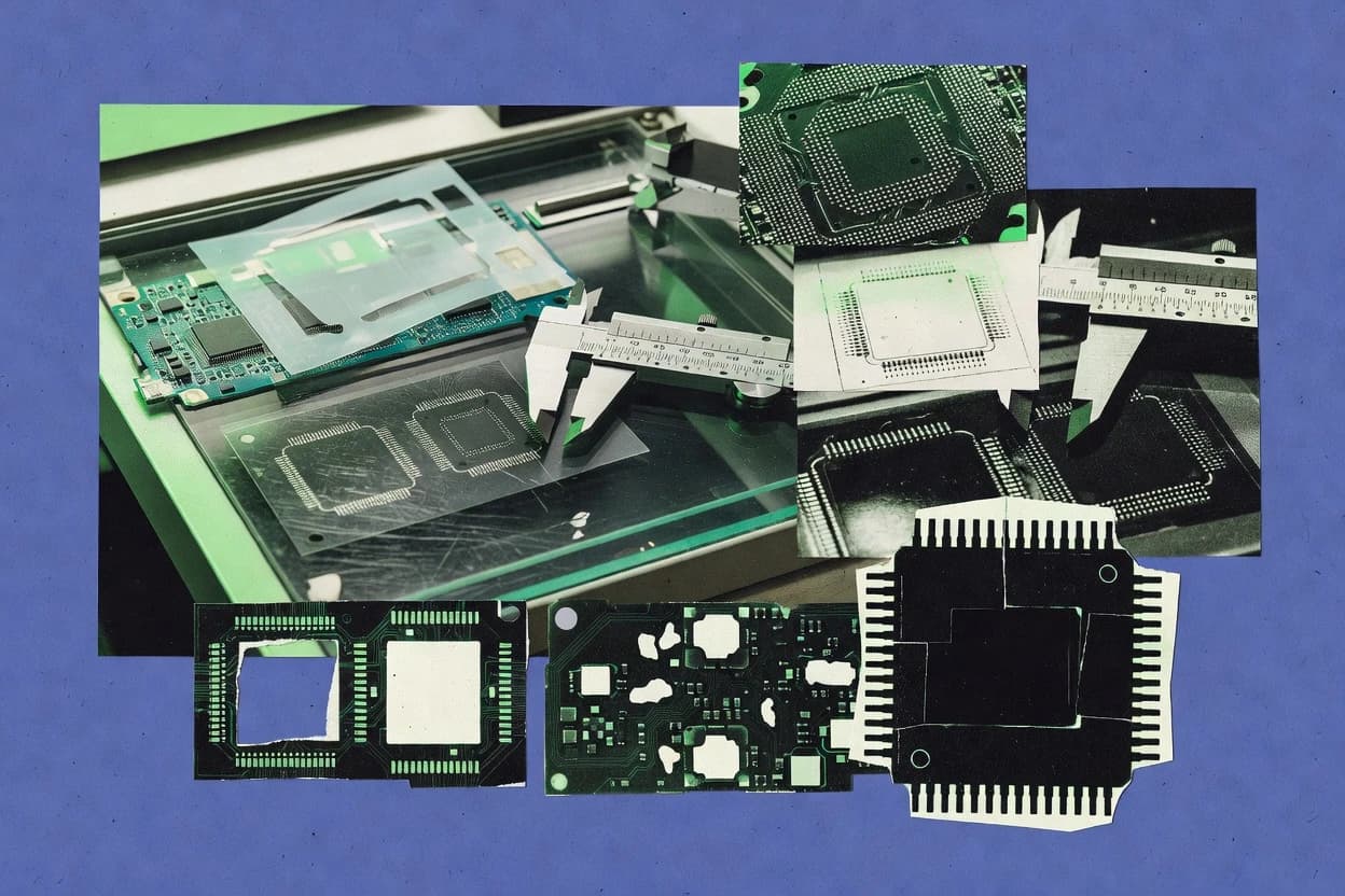
What Is Ic Package Design Software?
IC package design software creates and manages the geometric and data definitions that connect a chip package to PCB land patterns and manufacturing deliverables. These tools model package outlines, pin maps, pad and lead structures, keepouts, courtyard and assembly constraints, and linked 2D and 3D representations. Teams use them to reduce footprint inconsistency risk, automate constraint propagation, and generate outputs that support PCB layout and verification. Cadence Allegro Package Designer and Altium Designer represent the footprint-to-layout workflow style, while Ansys Electronics Desktop and COMSOL Multiphysics represent package validation through EM and multiphysics simulation.
Key Features to Look For
Tool selection should be driven by the exact deliverables needed for IC packaging, footprint reuse, and manufacturing-ready validation.
Database-managed package libraries with pin mapping
Cadence Allegro Package Designer excels at IC package footprint creation with pin mapping and database-managed library consistency. Altium Designer supports parameter-driven footprint generation and consistent pin and land patterns through its integrated library workflow.
Rule-driven footprint validation with courtyard and assembly constraints
Siemens PADS Professional focuses on rule-driven validation for package footprint and placement issues using courtyard and assembly-oriented constraints. Mentor Graphics xDX Designer extends this concept with constraint management that keeps package geometry and manufacturing-relevant layouts consistent.
3D-aware footprint visualization and mechanical placement support
Altium Designer provides integrated 3D package visualization that supports accurate body and courtyard placement. KiCad links footprints to 3D STEP models for mechanical fit checks, and Autodesk Fusion 360 supports parametric 3D assemblies for clearance validation around leads, bumps, and housings.
Template-based, model-driven constraint propagation for package variants
Mentor Graphics xDX Designer uses model-driven workflows and rules-based configuration to keep package geometry and constraints synchronized across views. xDX templates also accelerate variant package configuration when design teams require repeated reuse of structured rules.
Electromagnetic modeling with S-parameter extraction
Ansys Electronics Desktop enables full-wave 3D EM modeling of leadframes, substrates, and bump or solder interconnects. It generates S-parameter outputs for signal integrity and system co-simulation, which directly supports package-level performance verification.
Coupled thermal, structural, and EM multiphysics simulation
COMSOL Multiphysics combines electromagnetics with heat transfer and structural mechanics in one coupled workflow. It supports parametric sweeps and optimization studies to evaluate thermal gradients and strain impacts on electrical behavior.
How to Choose the Right Ic Package Design Software
Selecting the right tool comes down to whether the primary work is footprint and library automation, rule-based manufacturing validation, or package performance simulation.
Start with the deliverable: footprint data or package performance
If the main output is manufacturing-ready IC package footprints and pin maps that must hand off cleanly into PCB layout, start with Cadence Allegro Package Designer or Altium Designer. If the project priority is high-accuracy package interconnect performance using leadframes, substrates, and solder or bump structures, start with Ansys Electronics Desktop for EM and S-parameters.
Map your validation needs to rule systems and constraints
For manufacturing-focused teams that must catch courtyard and placement issues early, Siemens PADS Professional provides rule-driven footprint and courtyard verification. For teams needing automated synchronization between package geometry and manufacturing-relevant layouts, Mentor Graphics xDX Designer propagates constraints through template-driven design.
Choose library workflow strength based on reuse volume
Cadence Allegro Package Designer is built for producing many IC footprints with strict library standards and reusable pin and attribute mappings. Altium Designer supports parameter-driven footprint creation and 3D-aware component library workflows for repeatable reuse when large projects rely on controlled library structures.
Plan mechanical verification using 3D visualization and parametric CAD
Altium Designer supports 3D package visualization with accurate body and courtyard placement for layout-aware mechanical checking. KiCad links footprints to STEP models for mechanical fit checks, and Autodesk Fusion 360 provides parametric 3D assemblies with constraint-based clearances for lead, bump, and housing verification.
Add multiphysics simulation only when coupled behavior is required
If electrical and thermal-mechanical effects must be assessed together, COMSOL Multiphysics provides a coupled EM-thermal-structural workflow in one solve. For teams focusing on boundary conditions and meshing strategies for package geometry iterations, Ansys Electronics Desktop offers full-wave 3D EM with workflow integration across EM, circuit, and system analysis.
Who Needs Ic Package Design Software?
IC package design software targets teams that turn IC package definitions into manufacturable land patterns, mechanical representations, and simulation-ready models.
Teams producing many IC footprints with strict library and verification needs
Cadence Allegro Package Designer is the best fit because its IC package footprint creation emphasizes pin mapping and database-managed library consistency. Altium Designer also fits teams that need unified schematic-to-footprint-to-3D workflows with parameter-driven footprint creation.
Manufacturing-focused teams standardizing package footprints for PCB layout
Siemens PADS Professional aligns with manufacturing workflows because it provides rule-based validation for package footprint and courtyard considerations. Its library and reuse workflows support consistent IC package footprint definitions across projects.
Packaging teams needing template-driven automation for variant packages
Mentor Graphics xDX Designer fits packaging teams that require model-driven workflows and rules-based configuration. It uses templates and constraint propagation to keep package geometry and manufacturing-relevant layouts synchronized.
Teams validating package interconnect performance and system-level signal behavior
Ansys Electronics Desktop is designed for electromagnetic modeling that produces S-parameter outputs for signal integrity and system co-simulation. It supports complex geometries such as bumps, solder, and substrates for package-level interconnect verification.
Teams analyzing coupled thermal, structural, and EM impacts
COMSOL Multiphysics fits teams that need coupled electromagnetics with heat transfer and structural mechanics in a single simulation workflow. Its parametric sweeps and optimization studies support thermal gradient and strain tradeoff exploration.
Teams creating custom IC footprints and exporting manufacturing outputs
KiCad suits teams building custom IC footprints with repeatable fabrication outputs like Gerbers and drill files. Its footprint editor supports pad stack control and associates STEP 3D models for mechanical fit checks.
Teams designing mechanical package geometry and performing assembly verification
Autodesk Fusion 360 is a fit when mechanical package geometry and assemblies drive lead, bump, and housing clearance validation. It supports parametric 3D modeling and linked electronics documentation outputs for step-based mechanical package definitions.
Common Mistakes to Avoid
IC package projects often fail when tool selection mismatches the required deliverable depth, constraint rigor, or modeling workflow.
Treating footprint libraries as ad hoc assets instead of controlled data
IC teams that edit footprints without disciplined library standards can create data drift, which is explicitly a risk in Cadence Allegro Package Designer because it requires disciplined library standards for consistent reuse. Altium Designer reduces drift by supporting controlled library structures and parameter-driven footprint creation that standardizes pin mapping and land patterns.
Underestimating the effort needed to set up complex rule systems for new package types
Siemens PADS Professional can slow setup for new package types because constraint and rule complexity can require careful configuration. Mentor Graphics xDX Designer can also slow bespoke workflows when templates and complex constraints require upfront definition to avoid rework.
Expecting package editing in PCB-centric tools to be lightweight for advanced parameter workflows
Altium Designer can feel heavyweight for simple IC package editing and can require training to manage deep library automation. Cadence Allegro Package Designer can also feel heavy for small one-off package tweaks when advanced parameter and attribute workflows are involved.
Skipping mechanical verification by relying only on 2D footprints
KiCad requires correct STEP scaling and origins for reliable 3D mechanical fit checks, so mechanical validation needs attention to STEP model association details. Altium Designer and Autodesk Fusion 360 provide clearer mechanical placement and assembly verification through 3D package visualization and parametric assembly constraints.
How We Selected and Ranked These Tools
We evaluated every tool on three sub-dimensions. Features received a weight of 0.4, ease of use received a weight of 0.3, and value received a weight of 0.3. The overall rating uses the weighted average overall = 0.40 × features + 0.30 × ease of use + 0.30 × value. Cadence Allegro Package Designer separated from lower-ranked tools mainly through features strength in IC package footprint creation with pin mapping and database-managed library consistency, which directly improves reusable package data handoff reliability.
Frequently Asked Questions About Ic Package Design Software
Which tool best maintains a single source of truth for IC package footprints across many PCB projects?
What software supports a fully integrated schematic-to-PCB workflow while defining IC package 2D and 3D views?
Which option accelerates high-density IC package design using templates and automated constraint propagation?
When full-wave electromagnetic accuracy at the package level is required, which toolset is most direct?
Which tool is better for coupled thermal, structural, and electromagnetic evaluation of IC packages?
Which environment is best suited for manufacturing-focused IC land pattern checks like courtyard and assembly constraints?
What tool supports creating IC footprints with STEP-based 3D model linking and fabrication output generation for custom designs?
Which option is strongest for mechanical package geometry work with assembly context and electronics documentation linkage?
How do users avoid package-to-PCB pin mapping mistakes when generating land patterns?
Conclusion
After evaluating 8 manufacturing engineering, Cadence Allegro Package Designer stands out as our overall top pick — it scored highest across our combined criteria of features, ease of use, and value, which is why it sits at #1 in the rankings above.
Use the comparison table and detailed reviews above to validate the fit against your own requirements before committing to a tool.
Tools reviewed
Primary sources checked during evaluation.
Referenced in the comparison table and product reviews above.
Keep exploring
Comparing two specific tools?
Software Alternatives
See head-to-head software comparisons with feature breakdowns, pricing, and our recommendation for each use case.
Explore software alternatives→In this category
Manufacturing Engineering alternatives
See side-by-side comparisons of manufacturing engineering tools and pick the right one for your stack.
Compare manufacturing engineering tools→FOR SOFTWARE VENDORS
Not on this list? Let’s fix that.
Our best-of pages are how many teams discover and compare tools in this space. If you think your product belongs in this lineup, we’d like to hear from you—we’ll walk you through fit and what an editorial entry looks like.
Apply for a ListingWHAT THIS INCLUDES
Where buyers compare
Readers come to these pages to shortlist software—your product shows up in that moment, not in a random sidebar.
Editorial write-up
We describe your product in our own words and check the facts before anything goes live.
On-page brand presence
You appear in the roundup the same way as other tools we cover: name, positioning, and a clear next step for readers who want to learn more.
Kept up to date
We refresh lists on a regular rhythm so the category page stays useful as products and pricing change.