GITNUXSOFTWARE ADVICE
Manufacturing EngineeringTop 10 Best Electrical Circuit Software of 2026
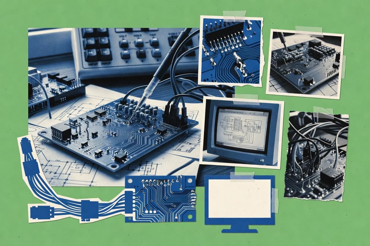
Compare the top Electrical Circuit Software tools with a ranked list of the best options, including Altium Designer and KiCad. Explore picks.

How we ranked these tools
Core product claims cross-referenced against official documentation, changelogs, and independent technical reviews.
Analyzed video reviews and hundreds of written evaluations to capture real-world user experiences with each tool.
AI persona simulations modeled how different user types would experience each tool across common use cases and workflows.
Final rankings reviewed and approved by our editorial team with authority to override AI-generated scores based on domain expertise.
Score: Features 40% · Ease 30% · Value 30%
Gitnux may earn a commission through links on this page — this does not influence rankings. Editorial policy
Editor’s top 3 picks
Three quick recommendations before you dive into the full comparison below — each one leads on a different dimension.
Altium Designer
Advanced Design Rule Check tied directly to schematic and PCB constraints
Built for hardware teams building complex PCB assemblies with tight design verification.
KiCad
Design Rules Check integrates with schematic and PCB constraints for early error detection
Built for engineers and hobbyists needing full PCB workflow without vendor lock-in.
Cadence OrCAD
Rule-based design checking linking schematic connectivity to PCB layout constraints
Built for teams converting schematics into manufacturable PCB layouts.
Related reading
- Manufacturing EngineeringTop 10 Best Electrical Circuit Design Software of 2026
- Manufacturing EngineeringTop 10 Best Electrical Circuit Builder Software of 2026
- Manufacturing EngineeringTop 10 Best Electrical Circuit Diagram Software of 2026
- Manufacturing EngineeringTop 10 Best Electrical Circuit Drawing Software of 2026
Comparison Table
This comparison table evaluates electrical circuit design and schematic capture tools, including Altium Designer, KiCad, Cadence OrCAD, Autodesk EAGLE, and Siemens EDA Xpedition. It highlights how each platform handles core workflows such as schematic entry, PCB layout integration, library management, and simulation support, so feature coverage can be compared side by side. The table also flags practical differences that affect tool choice, including licensing model, compatibility with common file formats, and suitability for small projects versus complex designs.
| # | Tool | Category | Overall | Features | Ease of Use | Value |
|---|---|---|---|---|---|---|
| 1 | Altium Designer Integrated electronics design suite for schematic capture, PCB layout, and rule-driven constraint checking for manufacturing-ready outputs. | EDA suite | 9.3/10 | 9.5/10 | 9.3/10 | 9.1/10 |
| 2 | KiCad Open-source EDA platform for schematic and PCB design with simulation-friendly workflows and export formats used by manufacturing tooling. | open-source EDA | 9.1/10 | 9.3/10 | 8.9/10 | 8.9/10 |
| 3 | Cadence OrCAD Schematic and PCB design environment used for electrical design validation workflows with outputs compatible with fabrication and assembly pipelines. | EDA suite | 8.8/10 | 9.0/10 | 8.5/10 | 8.8/10 |
| 4 | Autodesk EAGLE Schematic capture and PCB design tool that generates production artifacts like Gerbers for board fabrication and manufacturing handoff. | EDA for hardware | 8.5/10 | 8.4/10 | 8.5/10 | 8.5/10 |
| 5 | Siemens EDA Xpedition High-productivity PCB and system design environment aimed at complex electronic assemblies with constraint-centric design flows. | enterprise PCB | 8.2/10 | 8.3/10 | 7.9/10 | 8.4/10 |
| 6 | ANSYS Electronics Desktop Simulation platform for electrical and electromagnetic analysis across circuit and field solvers with repeatable engineering workflows. | simulation suite | 7.9/10 | 8.1/10 | 7.8/10 | 7.8/10 |
| 7 | COMSOL Multiphysics Multiphysics simulation platform that includes electrical interfaces for coupled electro-mechanical and field effects analysis. | multiphysics | 7.7/10 | 7.5/10 | 7.6/10 | 7.9/10 |
| 8 | Proteus Design Suite Schematic-driven electronics design and simulation suite that supports instrumented testing and virtual prototyping. | schematic simulation | 7.4/10 | 7.4/10 | 7.1/10 | 7.6/10 |
| 9 | Multisim NI schematic and simulation environment for analog electronics validation with measurement instruments modeled for test workflows. | circuit simulation | 7.1/10 | 6.8/10 | 7.4/10 | 7.2/10 |
| 10 | TINA-TI TI analog circuit simulation tool for quick SPICE modeling and evaluation of analog designs. | SPICE simulator | 6.8/10 | 7.0/10 | 6.6/10 | 6.7/10 |
Integrated electronics design suite for schematic capture, PCB layout, and rule-driven constraint checking for manufacturing-ready outputs.
Open-source EDA platform for schematic and PCB design with simulation-friendly workflows and export formats used by manufacturing tooling.
Schematic and PCB design environment used for electrical design validation workflows with outputs compatible with fabrication and assembly pipelines.
Schematic capture and PCB design tool that generates production artifacts like Gerbers for board fabrication and manufacturing handoff.
High-productivity PCB and system design environment aimed at complex electronic assemblies with constraint-centric design flows.
Simulation platform for electrical and electromagnetic analysis across circuit and field solvers with repeatable engineering workflows.
Multiphysics simulation platform that includes electrical interfaces for coupled electro-mechanical and field effects analysis.
Schematic-driven electronics design and simulation suite that supports instrumented testing and virtual prototyping.
NI schematic and simulation environment for analog electronics validation with measurement instruments modeled for test workflows.
TI analog circuit simulation tool for quick SPICE modeling and evaluation of analog designs.
Altium Designer
EDA suiteIntegrated electronics design suite for schematic capture, PCB layout, and rule-driven constraint checking for manufacturing-ready outputs.
Advanced Design Rule Check tied directly to schematic and PCB constraints
Altium Designer stands out for unified schematic-to-PCB engineering inside one toolchain that keeps design intent consistent. It supports hierarchical schematics, rules-driven PCB layout, and constraint-based design checking across electrical and physical domains. Advanced simulation and signal integrity workflows integrate into the same design environment, which reduces rework between capture and verification. Strong component and library management helps teams maintain reusable blocks for complex systems.
Pros
- Rules-driven PCB layout with constraint checking for fewer late-stage fixes
- Unified schematic and PCB database keeps nets, parameters, and footprints synchronized
- Powerful hierarchical design management for large multi-sheet projects
- Integrated signal integrity and simulation workflows for faster electrical verification
- Extensive component and library tooling for reusable design blocks
Cons
- Steep learning curve for constraint and advanced layout workflows
- Heavy projects can feel slow without careful setup
- Tool complexity increases overhead for simple one-off boards
- Version control and review still require disciplined team processes
- Customization depth can complicate consistent team standards
Best For
Hardware teams building complex PCB assemblies with tight design verification
More related reading
KiCad
open-source EDAOpen-source EDA platform for schematic and PCB design with simulation-friendly workflows and export formats used by manufacturing tooling.
Design Rules Check integrates with schematic and PCB constraints for early error detection
KiCad stands out with an integrated, open-source workflow for schematic capture, PCB layout, and fabrication outputs in a single toolchain. It supports hierarchical schematics, symbol libraries, and ERC rule checking to validate designs before layout. PCB design includes constraint-based design rules, interactive routing with differential pairs, and polygon pours for solid planes. Output generation covers Gerber files, drill data, and 3D visualization with a compatible library-driven component footprint system.
Pros
- Integrated schematic and PCB design in one project structure
- Hierarchical schematics with ERC for electrical rule validation
- Constraint-driven design rules enforce clearances and net classes
- Differential pair routing and interactive editing speed layout work
- Gerber, drill, and pick-and-place outputs for manufacturing handoff
Cons
- Complex library setup can slow first-time symbol and footprint creation
- Large projects can feel sluggish on weaker hardware
- Advanced automation requires manual scripting steps for some tasks
Best For
Engineers and hobbyists needing full PCB workflow without vendor lock-in
Cadence OrCAD
EDA suiteSchematic and PCB design environment used for electrical design validation workflows with outputs compatible with fabrication and assembly pipelines.
Rule-based design checking linking schematic connectivity to PCB layout constraints
Cadence OrCAD stands out for its tight workflow between schematic capture and PCB design tasks. It supports electrical design through schematic entry with component libraries, hierarchical design, and rule-based connectivity checks. OrCAD PCB tools enable layout creation with design rules, interactive routing, and fabrication-ready output generation. It is well suited for engineers who need an end-to-end circuit-to-board workflow inside one Cadence toolchain.
Pros
- Schematic capture with hierarchical design and robust connectivity checks
- PCB layout tools with interactive routing and design rule enforcement
- Library-driven component reuse for consistent electrical design workflows
Cons
- Complex projects often need careful rule setup to avoid reroute churn
- Workflow depth can feel heavyweight for very small, one-off circuits
- Simulation and advanced verification require separate specialized tooling
Best For
Teams converting schematics into manufacturable PCB layouts
Autodesk EAGLE
EDA for hardwareSchematic capture and PCB design tool that generates production artifacts like Gerbers for board fabrication and manufacturing handoff.
Schematic and PCB integration with netlist synchronization plus ERC and DRC validation
Autodesk EAGLE stands out for tight schematic and PCB design workflows with automatic net connectivity checks. It provides a full EDA toolchain for drawing schematics, authoring or importing component libraries, and laying out boards with routing tools and design-rule checks. Simulation is supported through linked SPICE workflows, which helps validate circuits before layout finalization. Data handling supports ERC and DRC to catch wiring errors and rule violations during iterative design.
Pros
- Schematic-to-PCB connectivity stays consistent with ERC and netlist-driven updates
- Library management supports creating symbols and footprints for repeatable parts
- Built-in routing and layer-aware layout tools speed up board construction
- Design-rule checks catch clearances and constraints before fabrication handoff
- SPICE simulation workflows enable early functional validation
Cons
- Complex high-speed or multi-physics analysis needs external tools
- Advanced automation requires scripting and can feel less guided than newer EDA suites
- Large projects can slow down during placement and rule-check passes
- Library compatibility with other EDA ecosystems can require manual conversion work
Best For
Teams needing reliable schematic-to-layout with strong rule checking and workflow discipline
Siemens EDA Xpedition
enterprise PCBHigh-productivity PCB and system design environment aimed at complex electronic assemblies with constraint-centric design flows.
Constraint-driven design rule checking that ties schematic intent to routing and layout verification
Siemens EDA Xpedition stands out for end-to-end schematic capture through board layout with tight integration between design data and constraints. It supports high-speed PCB design workflows with SI-aware routing, differential pair handling, and rule checks tied to physical implementation. The tool manages complex designs with hierarchical schematics, constraint-driven design rule enforcement, and revision control-friendly project structures for collaborative engineering. It also includes robust verification steps such as connectivity, DRC, and manufacturing readiness checks to reduce late-stage layout surprises.
Pros
- Strong schematic-to-layout integration with constraint-aware design rule checks
- High-speed routing features for differential pairs and signal integrity workflows
- Hierarchical design management supports large schematics and complex boards
- Connectivity and DRC verification reduce late layout rework
Cons
- Steeper learning curve than basic schematic-only tools
- Workflow setup for advanced constraints can be time-intensive
- Less ideal for lightweight personal projects needing minimal toolchain
Best For
Teams building constraint-driven PCB designs with high-speed considerations
ANSYS Electronics Desktop
simulation suiteSimulation platform for electrical and electromagnetic analysis across circuit and field solvers with repeatable engineering workflows.
Circuit-EM co-simulation with ANSYS field solutions for realistic interconnect modeling
ANSYS Electronics Desktop stands out for integrating circuit workflows with full-wave and multiphysics simulation in a single environment. It supports schematic capture and netlist-driven simulation for analog, RF, and power circuit design tasks. Designers can co-simulate with electromagnetic models to include field effects on interconnects and packages. The tool emphasizes verification through probe-based analysis, parameter sweeps, and automated design iteration across linked solvers.
Pros
- Tight integration of circuit and electromagnetic co-simulation
- Schematic and netlist workflows for analog and RF designs
- Parameter sweeps and automated iteration for design exploration
- Probe-based measurement tooling speeds debugging
Cons
- Complex setup when linking circuit models to EM geometry
- Large projects can demand significant compute resources
- RF circuit users may need stronger model management discipline
Best For
Teams needing EM-aware circuit simulation for RF and interconnect effects
COMSOL Multiphysics
multiphysicsMultiphysics simulation platform that includes electrical interfaces for coupled electro-mechanical and field effects analysis.
Multiphysics co-simulation connecting circuit networks with electromagnetic boundary-value problems
COMSOL Multiphysics stands out by combining circuit simulation with full multiphysics co-simulation across electromagnetics, thermal effects, and mechanics. Core capabilities include circuit modeling and solving with lumped elements and distributed-field coupling through its physics interfaces. Users can import geometries and material properties for electromagnetic boundary-value problems, then connect those results back into circuit networks for system-level behavior. The software supports parametric sweeps and time-dependent studies to evaluate transient and steady-state circuit performance.
Pros
- Strong multiphysics coupling between circuit models and electromagnetic field solvers
- Geometry-driven workflows for distributed effects tied to circuit behavior
- Parametric sweeps support fast sensitivity analysis across circuit parameters
- Time-dependent studies handle transient responses and dynamic interactions
- Extensive physics interfaces enable system modeling beyond pure circuits
Cons
- Setup can feel heavy when modeling circuits without field coupling
- Debugging mixed circuit and field models can be time-consuming
- Learning curve is steep due to many physics and solver options
Best For
Engineers modeling circuits coupled to EM fields and broader physical effects
Proteus Design Suite
schematic simulationSchematic-driven electronics design and simulation suite that supports instrumented testing and virtual prototyping.
Microcontroller integration with mixed-signal simulation and interactive stimulus testing
Proteus Design Suite stands out for combining schematic capture with simulation in a single workflow for electronics development. It supports SPICE-based circuit simulation, including mixed-signal work with microcontrollers and peripherals. Instrumentation tools enable waveform viewing, logic analysis, and stimulus creation for debugging behavior. Library-based design accelerates assembling common analog and digital building blocks into testable circuits.
Pros
- Tight schematic-to-simulation workflow reduces context switching during debug
- SPICE-based simulation supports detailed analog behavior and component-level testing
- Mixed-signal simulation links digital models with analog waveforms
- Logic and waveform viewers speed verification against expected signals
Cons
- Model accuracy depends on available component and MCU models
- Large designs can become slow to simulate and iterate
- Debugging complex timing issues may require careful stimulus configuration
Best For
Engineers simulating mixed-signal circuits with MCU behavior and waveform verification
Multisim
circuit simulationNI schematic and simulation environment for analog electronics validation with measurement instruments modeled for test workflows.
Virtual instrumentation probes link directly to simulation nodes during SPICE runs
Multisim stands out for its circuit-first workflow that pairs schematic capture with circuit simulation in one environment. It supports SPICE-based analysis with common analog and digital behaviors plus instrumentation-style measurement tools. Component libraries include selectable manufacturer-style parts and configurable models for repeatable design iteration. The tool is oriented toward rapid debugging of circuit behavior from the schematic through probe-based results.
Pros
- Integrated schematic capture with SPICE simulation for fast circuit iteration
- Rich virtual instruments for oscilloscope, multimeter, and waveform measurements
- Large component library with parameterized devices and models
Cons
- Digital logic design workflows feel weaker than dedicated HDL tools
- Model accuracy depends heavily on selected device SPICE parameters
- Complex mixed-signal schematics can become slow to simulate
Best For
Educators and engineers validating analog circuits with schematic-driven simulation
TINA-TI
SPICE simulatorTI analog circuit simulation tool for quick SPICE modeling and evaluation of analog designs.
TI integrated device model library for SPICE-accurate simulations
TINA-TI stands out for deep integration with TI parts models, making it practical for fast circuit simulation with manufacturer-accurate behaviors. The core workflow supports schematic-driven SPICE simulation with device models for analog electronics tasks like power conversion, amplifiers, and signal chains. Simulation runs include operating point, transient, frequency, and noise analyses, which cover most early-stage validation needs. TINA-TI also provides measurement and plotting tools that help interpret waveforms and compare scenarios across design iterations.
Pros
- TI device models reduce mismatch between simulated and real TI circuits
- Schematic-driven SPICE supports common analyses like transient and AC
- Waveform plotting and measurement tools streamline design iteration
- Library access speeds up building circuits from known TI components
Cons
- Heavy analog focus limits suitability for large digital systems
- Model accuracy depends on available TI components in the libraries
- Learning SPICE concepts is required for advanced setup
Best For
Engineers validating analog and power circuits using TI components
How to Choose the Right Electrical Circuit Software
This buyer's guide covers electrical circuit software for schematic capture, circuit simulation, and electronics-to-hardware workflows across Altium Designer, KiCad, Cadence OrCAD, Autodesk EAGLE, Siemens EDA Xpedition, ANSYS Electronics Desktop, COMSOL Multiphysics, Proteus Design Suite, Multisim, and TINA-TI. It maps each tool to the concrete engineering tasks it supports, such as design-rule checking, netlist-driven simulation, circuit-EM co-simulation, and mixed-signal MCU verification. The guide also explains how to choose based on verification depth, workflow coupling, and project scale.
What Is Electrical Circuit Software?
Electrical circuit software lets teams draw schematic designs and validate electrical behavior using rule checks and SPICE-style simulations, then connect that intent to PCB layout when manufacturing handoff is required. Tools like Altium Designer and Cadence OrCAD combine schematic connectivity with PCB layout constraints and design-rule checks so netlists, footprints, and layout constraints stay synchronized during iteration. Simulation-first tools like Proteus Design Suite and Multisim focus on schematic-driven circuit validation with virtual instrumentation and waveform inspection to debug circuit behavior quickly.
Key Features to Look For
The strongest results come from features that connect electrical intent to verification steps so errors are caught early and debugging stays tied to the schematic or constraints.
Constraint-linked design-rule checking across schematic and PCB
Altium Designer provides an advanced Design Rule Check tied directly to schematic and PCB constraints, which targets late-stage fixes by enforcing intent before layout reaches fabrication readiness. KiCad, Cadence OrCAD, Autodesk EAGLE, Siemens EDA Xpedition, and Autodesk EAGLE also integrate connectivity and constraint validation using ERC and DRC style checks that surface wiring and clearance issues during iterative design.
Schematic-to-PCB netlist synchronization that keeps electrical connectivity consistent
Altium Designer keeps nets, parameters, and footprints synchronized in a unified schematic and PCB database so connectivity remains consistent from capture to constraint checking. Autodesk EAGLE specifically emphasizes schematic and PCB integration with netlist synchronization plus ERC and DRC validation, which reduces the chance of mismatched connectivity during placement and routing.
Hierarchical project structure with ERC and connectivity checks for multi-sheet designs
Altium Designer and Cadence OrCAD support hierarchical design management so large multi-sheet projects remain navigable and connectivity checks stay organized. KiCad also uses hierarchical schematics with ERC rule checking so electrical rule validation happens before layout constraints are enforced.
Simulation that is driven from the schematic with measurement-grade inspection
Proteus Design Suite pairs schematic-driven SPICE simulation with instrumentation tools for waveform viewing, logic analysis, and stimulus creation, which speeds verification of mixed-signal circuits. Multisim adds virtual instrumentation probes that link directly to simulation nodes during SPICE runs, which helps validate analog behavior with oscilloscope and multimeter style measurements.
Component model libraries that reflect real device behavior for faster analog validation
TINA-TI is built around TI integrated device model libraries, which makes transient, AC, operating point, and noise analyses practical for TI-based analog and power work. ANSYS Electronics Desktop focuses on netlist-driven circuit workflows that link to electromagnetic models for more realistic interconnect effects in addition to circuit behavior.
EM-aware co-simulation or multiphysics coupling for interconnect and field effects
ANSYS Electronics Desktop supports circuit-EM co-simulation with ANSYS field solutions so interconnect and packaging effects can be included in circuit verification. COMSOL Multiphysics enables circuit networks to connect to electromagnetic boundary-value problems through multiphysics coupling, while Siemens EDA Xpedition emphasizes constraint-driven routing with SI-aware handling for high-speed signals.
How to Choose the Right Electrical Circuit Software
Selection should start with the verification target, then match the tool that ties electrical design to the required constraint checks, simulation fidelity, and measurement workflow.
Choose the verification depth: PCB rule enforcement versus circuit-first simulation
If the deliverable is a manufacturable PCB, Altium Designer and KiCad excel because both integrate constraint-driven design-rule checking into a schematic-plus-PCB workflow. If the priority is rapid electrical validation with probes and waveforms, Proteus Design Suite and Multisim provide schematic-driven SPICE simulation with instrumentation-style viewing that keeps debugging close to the circuit behavior.
Verify that schematic intent and layout constraints stay synchronized
Altium Designer and Autodesk EAGLE keep schematic connectivity aligned with PCB work using netlist synchronization plus ERC and DRC validation, which supports fewer rework loops. Cadence OrCAD also links schematic connectivity to PCB constraints with rule-based design checking so connectivity and routing decisions are enforced together.
Match the tool to project scale and design structure needs
For large multi-sheet projects, Altium Designer and Cadence OrCAD provide hierarchical design management and robust connectivity checks that keep verification structured. KiCad supports hierarchical schematics with ERC validation but can slow down on weaker hardware, so performance planning matters for larger boards.
Pick the right simulation model fidelity for the problem domain
For TI-focused analog and power validation, TINA-TI is practical because it includes TI integrated device model libraries and supports analyses like transient, frequency, and noise. For RF and interconnect effects, ANSYS Electronics Desktop is built for circuit-EM co-simulation using ANSYS field solutions, which is a different fidelity level than schematic-only SPICE validation.
Use co-simulation or multiphysics only when the system coupling is actually required
COMSOL Multiphysics is the better fit when circuits must connect to electromagnetic, thermal, and mechanical effects through physics interfaces and time-dependent studies. Siemens EDA Xpedition fits when high-speed PCB routing needs SI-aware handling and constraint-centric verification tied to physical implementation rather than full field-coupled simulation.
Who Needs Electrical Circuit Software?
Different electrical circuit software tools serve different engineering workflows, from PCB manufacturing rule checking to instrumented mixed-signal debugging and EM-aware simulation.
Hardware teams building complex PCB assemblies with tight verification loops
Altium Designer is designed for complex PCB assemblies with advanced Design Rule Check tied directly to schematic and PCB constraints, which targets fewer late-stage layout fixes. Siemens EDA Xpedition also fits teams focused on constraint-driven PCB designs with connectivity, DRC, and manufacturing readiness checks tied to routing and layout verification.
Engineers who need a complete open workflow for schematic and PCB deliverables
KiCad is built for schematic capture, PCB layout, and fabrication outputs in one toolchain using ERC, constraint-driven PCB design rules, and manufacturing exports like Gerber and drill data. Its integrated design-rule checking helps validate errors early before final fabrication handoff.
Teams converting schematics into manufacturable PCB layouts inside a single environment
Cadence OrCAD emphasizes an end-to-end circuit-to-board workflow using hierarchical schematic connectivity checks and rule-based PCB layout enforcement. Autodesk EAGLE also supports reliable schematic-to-layout with netlist synchronization plus ERC and DRC validation.
Engineers validating analog, power, or device-specific circuits quickly
TINA-TI is optimized for analog and power circuit validation with TI integrated device model libraries and support for operating point, transient, frequency, and noise analyses. Multisim supports rapid analog debugging with SPICE simulation plus virtual instrumentation probes linked directly to simulation nodes.
Engineers working on mixed-signal designs with MCU behavior and waveform verification
Proteus Design Suite supports mixed-signal simulation with microcontroller integration, instrumented testing tools, and interactive stimulus creation for waveform and logic analysis. This combination supports debugging circuit behavior against expected signals without switching between separate instrument tools.
Teams needing EM-aware circuit simulation for RF and interconnect effects
ANSYS Electronics Desktop provides circuit-EM co-simulation with ANSYS field solutions so field effects on interconnects and packages are included in circuit verification. COMSOL Multiphysics supports multiphysics coupling that connects circuit networks to electromagnetic boundary-value problems and time-dependent studies.
Common Mistakes to Avoid
Common selection and implementation errors usually come from choosing a tool that does not connect the needed design checks or simulation fidelity to the schematic or PCB constraints used in the project.
Choosing schematic-only simulation when PCB constraint verification is required
Proteus Design Suite and Multisim focus on circuit simulation and virtual instrumentation, so they do not provide the same schematic-plus-PCB constraint checking workflow found in Altium Designer or KiCad. For manufacturable PCB work, Altium Designer, Cadence OrCAD, and Siemens EDA Xpedition keep electrical intent linked to routing and layout verification through rule-based or constraint-driven checks.
Ignoring design-rule alignment between schematic connectivity and PCB constraints
Using Autodesk EAGLE without maintaining disciplined ERC and DRC validation increases the chance of clearance and constraint issues reaching later layout stages. Altium Designer and Cadence OrCAD reduce this risk by tying rule-based design checking directly to schematic connectivity and PCB constraints.
Under-scoping device model fidelity for analog and power validation
Using general-purpose circuit models without manufacturer-aligned libraries can cause mismatch when device behavior matters, which is why TINA-TI is specialized around TI integrated device model libraries. For broader EM-sensitive interconnect work, ANSYS Electronics Desktop avoids relying only on schematic models by including circuit-EM co-simulation with ANSYS field solutions.
Selecting multiphysics or EM co-simulation for problems that do not require field coupling
COMSOL Multiphysics is strong for circuits coupled to electromagnetic, thermal, and mechanical effects, but setup and debugging mixed field and circuit models can be time-consuming. For high-speed PCB routing needs without full field coupling, Siemens EDA Xpedition provides SI-aware routing and constraint-centric verification focused on physical implementation.
How We Selected and Ranked These Tools
we evaluated every tool on three sub-dimensions. Features received weight 0.4, ease of use received weight 0.3, and value received weight 0.3. The overall rating is the weighted average computed as overall = 0.40 × features + 0.30 × ease of use + 0.30 × value. Altium Designer separated itself by combining high feature depth in constraint-linked PCB verification with a tightly integrated schematic-to-PCB database, which supported fewer late-stage fixes through its advanced Design Rule Check tied directly to schematic and PCB constraints.
Frequently Asked Questions About Electrical Circuit Software
Which toolchain offers the tightest schematic-to-PCB consistency for complex designs?
Altium Designer keeps electrical intent and PCB constraints in one workflow so design rules propagate from schematic through layout. Cadence OrCAD also supports a connected flow with rule-based connectivity checks that link schematic relationships to PCB routing constraints.
Which software best supports open-source PCB workflows with fabrication outputs in one place?
KiCad provides an integrated schematic-to-PCB flow with ERC validation and constraint-based DRC. It generates Gerber files, drill data, and 3D visualization using library-driven footprints, which reduces tool hopping.
What tool is best for end-to-end circuit-to-board work when connectivity checking must follow layout constraints?
Cadence OrCAD focuses on a rule-based schematic-to-PCB process where connectivity checks map into PCB design rule enforcement. Altium Designer offers similarly strong rule checking, but OrCAD is purpose-built for converting schematics into manufacturable PCB layouts inside the Cadence toolset.
Which package is strongest for high-speed PCB design that accounts for SI-aware routing and differential pairs?
Siemens EDA Xpedition supports high-speed workflows with SI-aware routing and differential pair handling tied to board implementation rules. Altium Designer also integrates advanced SI workflows, including signal integrity verification tied to schematic and PCB constraints.
Which circuit software is best when electromagnetic interconnect effects must be included during circuit simulation?
ANSYS Electronics Desktop enables circuit co-simulation with field solutions so interconnect behavior can feed back into circuit responses. COMSOL Multiphysics similarly couples circuit networks with electromagnetic boundary-value problems and supports time-dependent and parametric studies for transient behavior.
Which tool is most effective for mixed-signal circuit debugging with waveform viewing and stimulus creation?
Proteus Design Suite combines schematic capture with SPICE-based mixed-signal simulation and includes instrumentation tools for waveform viewing and logic analysis. Multisim also provides probe-based measurements directly tied to SPICE nodes, which supports rapid circuit behavior validation.
Which option is best for education and rapid analog verification using schematic-driven probes?
Multisim is built around circuit-first schematic-driven simulation with instrumentation-style probes linked to simulation nodes. Proteus Design Suite is also suitable for analog and MCU-adjacent mixed-signal work because it adds interactive stimulus testing for debugging behavior.
How do SPICE workflows differ across tools when device models and accuracy matter for power electronics and amplifiers?
TINA-TI emphasizes manufacturer-accurate TI device models so operating point, transient, frequency, and noise analyses match TI component behavior. Autodesk EAGLE supports linked SPICE workflows for validation, but TINA-TI’s TI-focused model library is designed to keep early-stage circuit validation aligned with TI parts.
What is the most common workflow problem that rule checking helps solve when designs fail at the wiring or layout stage?
Schematic-to-layout mismatch often causes open nets, incorrect connectivity, or rule violations that only show up after routing. KiCad’s ERC and design rules check catch issues earlier across schematic and PCB constraints, while Altium Designer and Autodesk EAGLE use netlist synchronization plus ERC and DRC validation to prevent late-stage surprises.
Conclusion
After evaluating 10 manufacturing engineering, Altium Designer stands out as our overall top pick — it scored highest across our combined criteria of features, ease of use, and value, which is why it sits at #1 in the rankings above.
Use the comparison table and detailed reviews above to validate the fit against your own requirements before committing to a tool.
Tools reviewed
Referenced in the comparison table and product reviews above.
Keep exploring
Comparing two specific tools?
Software Alternatives
See head-to-head software comparisons with feature breakdowns, pricing, and our recommendation for each use case.
Explore software alternatives→In this category
Manufacturing Engineering alternatives
See side-by-side comparisons of manufacturing engineering tools and pick the right one for your stack.
Compare manufacturing engineering tools→FOR SOFTWARE VENDORS
Not on this list? Let’s fix that.
Our best-of pages are how many teams discover and compare tools in this space. If you think your product belongs in this lineup, we’d like to hear from you—we’ll walk you through fit and what an editorial entry looks like.
Apply for a ListingWHAT THIS INCLUDES
Where buyers compare
Readers come to these pages to shortlist software—your product shows up in that moment, not in a random sidebar.
Editorial write-up
We describe your product in our own words and check the facts before anything goes live.
On-page brand presence
You appear in the roundup the same way as other tools we cover: name, positioning, and a clear next step for readers who want to learn more.
Kept up to date
We refresh lists on a regular rhythm so the category page stays useful as products and pricing change.