GITNUXSOFTWARE ADVICE
Manufacturing EngineeringTop 10 Best Design Circuit Board Software of 2026
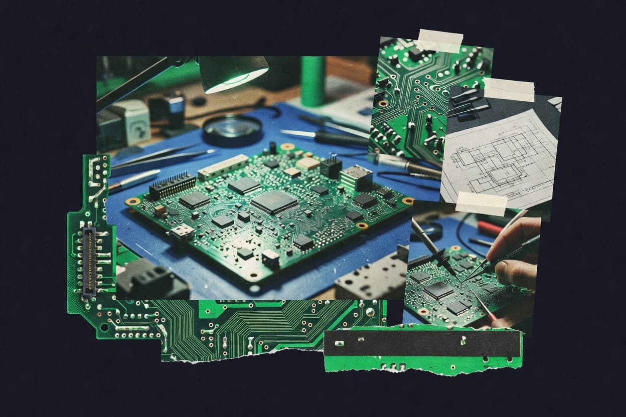
Compare the top 10 Design Circuit Board Software picks. Altium Designer, OrCAD, and KiCad rank for faster PCB design. Explore now.

How we ranked these tools
Core product claims cross-referenced against official documentation, changelogs, and independent technical reviews.
Analyzed video reviews and hundreds of written evaluations to capture real-world user experiences with each tool.
AI persona simulations modeled how different user types would experience each tool across common use cases and workflows.
Final rankings reviewed and approved by our editorial team with authority to override AI-generated scores based on domain expertise.
Score: Features 40% · Ease 30% · Value 30%
Gitnux may earn a commission through links on this page — this does not influence rankings. Editorial policy
Editor’s top 3 picks
Three quick recommendations before you dive into the full comparison below — each one leads on a different dimension.
Altium Designer
Integrated PCB 3D visualization and clearance checking tied to design rules
Built for complex PCB design teams needing integrated workflow control.
OrCAD / PSpice
Editor pickPSpice analog and mixed-signal simulation with device-model-based analysis
Built for teams needing robust analog simulation plus disciplined PCB layout workflows.
KiCad
Editor pickUnified KiCad project workflow with footprint-linking and rule-driven DRC
Built for engineers needing a full PCB toolchain with strong control over rules.
Related reading
Comparison Table
This comparison table evaluates major design circuit board software tools used for schematic capture, PCB layout, and simulation workflows, including Altium Designer, OrCAD with PSpice, KiCad, Cadence Allegro, and Mentor Graphics PADS. It highlights key differences across feature coverage, design file ecosystem, simulation and automation capabilities, and integration patterns that affect real project throughput. The result is a side-by-side reference for selecting the best fit for specific tooling, licensing constraints, and technical requirements.
Altium Designer
professional PCB CADAltium Designer is a PCB design and schematic capture application with library management, rules-based constraints, and manufacturing data output for complex assemblies.
Integrated PCB 3D visualization and clearance checking tied to design rules
Altium Designer stands out for deeply integrated schematic, PCB, and library workflows in a single, highly connected authoring environment. It supports advanced PCB design with 2D and 3D visualization, robust constraint-driven rules, and mature routing and placement tooling for high-density boards.
It also includes extensive interoperability for versioned data, simulation and model integration, and downstream manufacturing handoff. The software excels when projects need consistent design intent from schematic through fabrication outputs.
- +Strong constraint-driven design rules across schematics and PCB layouts
- +Deep 2D plus 3D PCB visualization for fit and clearance checks
- +Powerful library and component model management for reusable designs
- +Reliable fabrication output generation with structured documentation data
- –Steep learning curve from dense options and workflow complexity
- –Heavy projects can demand substantial system resources for smooth editing
- –Some collaboration workflows rely on external process discipline
Best for: Complex PCB design teams needing integrated workflow control
More related reading
OrCAD / PSpice
schematic plus PCBOrCAD combines schematic capture and PCB layout workflows with integrated simulation via PSpice for electronics design and verification.
PSpice analog and mixed-signal simulation with device-model-based analysis
OrCAD and PSpice stand out by pairing schematic capture with a mature SPICE simulation engine tailored to mixed analog and digital verification workflows. The toolset supports PCB design activities through constraint-driven layout, component placement and routing, and library-based design reuse across projects.
PSpice models and analyses help validate circuit behavior before layout, which reduces iteration cycles when design intent is stable. The overall workflow is most productive for teams that already think in terms of netlists, device models, and simulation-driven checks alongside PCB layout.
- +Strong PSpice simulation coverage for analog and mixed-signal circuit checks
- +Tight schematic-to-simulation workflow using netlist-ready design objects
- +Constraint-driven PCB layout supports repeatable rules-based routing
- +Library and project reuse reduces redesign for common component ecosystems
- –Learning curve is steep for simulation setup and model management
- –Modern interface and workflow conveniences lag behind newer EDA tools
- –Cross-tool integration feels less streamlined for highly automated flows
Best for: Teams needing robust analog simulation plus disciplined PCB layout workflows
KiCad
open-source PCB CADKiCad provides open-source schematic capture and PCB layout with component libraries, ERC/DRC checks, and export for fabrication and assembly.
Unified KiCad project workflow with footprint-linking and rule-driven DRC
KiCad stands out as a complete open-source EDA suite that spans schematic capture through PCB layout and manufacturing output. It provides a full toolchain for board design including netlist-driven linking, DRC rule checking, 2D and 3D visualization, and Gerber plus manufacturing file generation.
Users can manage libraries for symbols and footprints and maintain versioned design data for repeatable builds. The workflow is powerful for detailed PCB work, but it relies on manual setup for some multi-user and automation-heavy processes.
- +End-to-end flow from schematic capture to manufacturing outputs without third-party glue
- +Strong connectivity and netlist synchronization between schematic and PCB
- +Customizable DRC and design rules support consistent board quality
- +Integrated 3D viewer helps validate clearances and packaging geometry
- –Editing and constraint workflows can feel slower than mainstream commercial EDA
- –Advanced automation often requires scripting or external tooling
- –Library quality depends heavily on curated symbols and footprints
Best for: Engineers needing a full PCB toolchain with strong control over rules
Cadence Allegro
enterprise PCB CADCadence Allegro PCB Design targets high-speed and large-scale board design with advanced routing, constraint-driven flows, and manufacturing-ready outputs.
Allegro PCB Editor constraint-driven routing and comprehensive rule checking
Cadence Allegro stands out for its deep, enterprise-grade PCB implementation flow that covers place, route, and signoff with tight constraint control. The platform supports advanced connectivity management through Allegro Design Entry and Allegro PCB Editor workflows, which makes it strong for complex netlists and large designs.
Constraint-driven routing, robust rule checking, and integration with downstream analysis keep design intent consistent across layout, verification, and handoff. The toolset is geared toward professional teams that need predictable manufacturing outcomes for high-density boards.
- +Constraint-driven routing with strong design intent preservation
- +Mature connectivity, rule checking, and ECO workflows for large boards
- +Signoff-oriented flow integration across implementation and verification
- –Steep learning curve for setup, constraints, and advanced automation
- –Workflow depth can slow iteration for small or early-stage prototypes
- –Requires careful library and process configuration to avoid rework
Best for: Large, complex PCB teams needing rule-driven implementation and signoff stability
Mentor Graphics PADS
PCB design suitePADS is a PCB design suite that supports schematic and layout tasks with design-rule checking and manufacturing exports.
Constraint-driven DRC and routing guidance within PCB layout
Mentor Graphics PADS stands out with mature PCB design workflows built for high-throughput schematic-to-layout projects. It supports schematic capture, PCB layout, and library-driven design management with strong signal routing and constraint handling.
The tool integrates tightly with Mentor’s broader EDA ecosystem, which helps teams standardize processes across design, verification, and downstream manufacturing deliverables. For complex boards, it emphasizes productivity features like reusable blocks, templates, and robust DRC-driven iteration loops.
- +Strong schematic-to-layout integration for faster routing from known intent
- +Powerful constraints and DRC support for cleaner board iteration cycles
- +Reusable design blocks and library workflows improve team standardization
- –User interface can feel dense compared with newer CAD tools
- –Advanced flow setup takes time for teams migrating existing practices
- –Cross-tool workflow depth depends on how the broader Mentor toolchain is used
Best for: Teams building complex PCBs needing repeatable workflows and rigorous DRC
EPLAN Electric P8
schematic and documentationEPLAN Electric P8 is a schematic and wiring design system that generates consistent engineering documentation for manufacturing packages.
EPLAN Electric P8 macro and template-driven systematic circuit documentation generation
EPLAN Electric P8 stands out for a rule-driven data model that connects schematic components to documentation and downstream wiring views. The software supports full electrical circuit design with macros, component management, and systematic creation of terminals, cross-references, and harness documentation.
Strong interoperability shows up through EPLAN APIs and standard exchange formats for engineering data reuse across projects and disciplines. The overall workflow emphasizes standardized document sets, structured project management, and automation to reduce manual rework.
- +Tight link between symbols, tag data, terminals, and documentation outputs reduces inconsistencies
- +Configurable macros and templates enable repeatable schematic and terminal workflows
- +Advanced search and cross-reference navigation speeds up large project reviews
- –Toolchain complexity grows quickly for teams without prior EPLAN data-model setup
- –Learning curve is steep for automation rules, master data, and project structure
- –Interface can feel rigid for custom workflows that break from standard documentation
Best for: Engineering teams standardizing electrical schematics, terminals, and documentation automation at scale
ExpressPCB
web-based PCB designExpressPCB offers an online PCB design tool that generates production-ready files for fabricators and assembly planning.
Schematic-to-PCB workflow that drives an expedited, layout-first design process
ExpressPCB focuses on fast PCB layout by turning a schematic workflow into manufacturable board files quickly. The tool provides guided design steps, interactive placement, and an editor tuned for trace routing and board dimension control.
It supports common PCB needs like layers, design rules, and export-ready outputs geared toward board fabrication. Depth for advanced custom automation or complex multi-variant projects is more limited than in fully featured EDA suites.
- +Guided layout flow reduces setup time for basic PCB builds
- +Interactive routing tools support quick trace creation and adjustments
- +Export outputs are tailored for turning designs into fabrication-ready files
- –Advanced design-rule and constraint modeling is less comprehensive than top EDA tools
- –Library and component management options are narrower for large projects
- –Complex multi-board or multi-variant workflows feel harder to maintain
Best for: Small teams needing quick PCB layouts and fabrication-ready outputs
EasyEDA
cloud PCB CADEasyEDA is a browser-based schematic and PCB design platform with integrated library assets and export for manufacturing.
EasyEDA auto-links footprints to symbols to prevent schematic-to-PCB inconsistencies
EasyEDA stands out for merging schematic capture and PCB layout in a single web workflow with immediate cross-highlighting between design views. It supports hierarchical schematics, interactive part libraries, and Gerber and fabrication output generation for board manufacturing.
The platform also includes simulation-oriented tools and tight footprint management to reduce common symbol-to-footprint mismatches. Collaboration features center on shared projects with revision history for teams iterating on the same board files.
- +Web-based schematic and PCB layout keep design changes synced instantly
- +Extensive component and footprint library reduces part-creation overhead
- +Gerber, drill, and fabrication outputs are generated from the same workspace
- +Interactive ERC and DRC workflows catch wiring and footprint issues early
- –Advanced layout control is less granular than desktop pro tools
- –Large designs can feel slower due to browser-centric performance limits
- –Some simulation depth is limited compared to dedicated simulation suites
Best for: Small teams producing production-ready boards with browser-based workflows
Autodesk Fusion Electronics
prototyping PCB CADFusion Electronics supports schematic capture and PCB layout for electronics prototyping with export of fabrication outputs.
Fusion Electronics integration with Autodesk Fusion for unified mechanical-electrical workflows.
Autodesk Fusion Electronics stands out by integrating electronic design workflows with Autodesk Fusion’s CAD-centric environment. It supports schematic capture and PCB layout with a rules-driven design approach for connectivity and board constraints.
The tool also ties into Autodesk’s broader data model so teams can manage design assets across mechanical and electronics activities. Real-time collaboration and deep manufacturing outputs are more limited than specialized PCB-only suites, which narrows its fit for highly production-focused flows.
- +Tight linkage between electronics layout and Fusion-based mechanical design
- +Rules-driven net and constraint handling reduces manual routing errors
- +Integrated project data management helps keep ECAD and CAD consistent
- +Works well for mixed teams that design enclosures and circuits together
- –PCB specialization depth is weaker than dedicated ECAD platforms
- –Complex high-volume manufacturing workflows need extra toolchains
- –Learning curve rises for users focused only on conventional PCB editors
Best for: Product teams aligning PCB layout with mechanical CAD and design review.
CircuitMaker
free PCB CADCircuitMaker delivers a PCB design environment with schematic capture and board layout for electronics development and file export.
Interactive PCB routing with constraint-driven design rules
CircuitMaker focuses on PCB design for small electronics projects with a KiCad-like workflow and an interface tuned for schematic capture and layout. It supports symbol and footprint libraries, constraint-based design rules, and interactive routing and placement for multi-layer boards.
The tool also includes basic collaboration-style outputs like Gerber and drill exports for fabrication handoff. Its capability ceiling shows up in advanced manufacturing workflows and high-end ECAD automation compared with larger professional suites.
- +Schematic-to-layout workflow feels fast for hobby and small-team boards
- +Design rules and interactive routing support practical iterative PCB changes
- +Exports for fabrication use common outputs like Gerber and drill files
- –Limited high-end ECAD automation compared with premium commercial tools
- –Library management can become cumbersome for large component catalogs
- –Complex multi-board projects need careful setup to stay organized
Best for: Hobbyists and small teams needing reliable PCB layout without enterprise tooling
How to Choose the Right Design Circuit Board Software
This buyer’s guide covers how to choose Design Circuit Board Software tools using concrete capabilities from Altium Designer, OrCAD / PSpice, KiCad, and Cadence Allegro. It also maps priorities to the strengths and limitations of Mentor Graphics PADS, EPLAN Electric P8, ExpressPCB, EasyEDA, Autodesk Fusion Electronics, and CircuitMaker. The sections below focus on schematic capture, PCB layout, rules and verification, visualization, and manufacturing and documentation handoff.
What Is Design Circuit Board Software?
Design Circuit Board Software is the electronic design automation workflow that combines schematic capture, PCB layout, and rule-based checks so boards can move from design intent to fabrication-ready outputs. These tools prevent errors by linking schematic netlists to PCB connectivity and running DRC and ERC checks, then generating manufacturing file sets like Gerber plus drill. Some products also add 3D visualization for fit and clearance validation, and others extend into simulation or documentation automation. In practice, Altium Designer targets integrated schematic, PCB, and library workflows for complex assemblies, while KiCad provides an open toolchain that spans schematic, PCB, DRC, and export without relying on third-party glue tools.
Key Features to Look For
The best tool matches the design risks and handoff needs that matter for the project size, team process, and verification scope.
Constraint-driven design rules across schematic and PCB
Look for rules that stay consistent from design intent to placement and routing constraints. Altium Designer emphasizes strong constraint-driven design rules across schematics and PCB layouts, and Cadence Allegro delivers constraint-driven routing with robust rule checking. Mentor Graphics PADS adds constraint-driven DRC and routing guidance inside the PCB layout stage.
Integrated 2D and 3D PCB visualization with clearance checking
Choose a tool that can validate physical fit and clearance without exporting to a separate system. Altium Designer provides deep 2D plus 3D PCB visualization tied to design rules for clearance checking. KiCad also includes an integrated 3D viewer to validate clearances and packaging geometry during PCB work.
Tight schematic-to-netlist-to-PCB connectivity synchronization
Connectivity errors slow down layout and create rework when manufacturing files no longer match the intended circuit. KiCad emphasizes strong connectivity and netlist synchronization between schematic and PCB. EasyEDA uses auto-linking between footprints and symbols to prevent schematic-to-PCB inconsistencies.
Manufacturing-ready outputs and structured fabrication handoff data
Select software that produces fabrication file sets directly from the same workspace used for design verification. Altium Designer is built around reliable fabrication output generation with structured documentation data. ExpressPCB and EasyEDA both generate export outputs tailored for turning designs into fabrication-ready files from the design environment.
Verification depth that matches the circuit type
If the work depends on analog or mixed-signal behavior, simulation depth becomes a core layout decision factor. OrCAD / PSpice pairs schematic capture with PSpice analog and mixed-signal simulation using device-model-based analysis. Tools like KiCad focus on ERC and DRC and provide a complete PCB toolchain without placing the simulation center of gravity on the same path.
Workflow support for large designs and signoff readiness
High-density, large-net-count projects need routing predictability, rule coverage, and signoff workflows. Cadence Allegro targets enterprise-grade place, route, and signoff with mature connectivity management and ECO-oriented workflows. Mentor Graphics PADS supports complex boards with reusable blocks, templates, and rigorous DRC-driven iteration loops.
How to Choose the Right Design Circuit Board Software
A selection framework starts by matching verification and workflow depth to project scale and then checks whether the tool’s handoff path matches the target manufacturing and documentation process.
Match schematic-to-layout integrity controls to the most common failure mode
If the most frequent issue is symbol-to-footprint mismatch, EasyEDA’s auto-linking between footprints and symbols prevents schematic-to-PCB inconsistencies. If the project needs end-to-end schematic-to-PCB control with footprint linking and rule-driven DRC, KiCad provides a unified project workflow built around netlist-driven linking. If the project involves complex assemblies where design intent must be consistent across capture and layout, Altium Designer ties constraint-driven rules and fabrication handoff to the same connected authoring environment.
Choose verification scope based on whether behavior simulation is part of signoff
For analog and mixed-signal checks that require device-model-based analysis, OrCAD / PSpice combines schematic capture with PSpice simulation tied to the netlist-ready design objects. For board layout correctness and physical clearance validation, KiCad and Altium Designer emphasize ERC and DRC plus 3D viewing for fit and clearance checks. For strict rule-driven routing stability on complex high-density boards, Cadence Allegro and Mentor Graphics PADS provide comprehensive rule checking tied to constraint-driven routing.
Select the physical validation workflow that fits the team’s enclosure and mechanical reality
When mechanical-electrical consistency matters, Autodesk Fusion Electronics integrates PCB layout with Autodesk Fusion so design changes align with enclosure and mechanical design review. When fit and clearance checks must happen in the electrical tool itself, Altium Designer offers integrated PCB 3D visualization tied to design rules. KiCad’s 3D viewer supports clearance validation for packaging geometry without leaving the PCB workflow.
Pick the handoff model that matches fabrication and documentation expectations
If the process requires structured documentation data and reliable fabrication output generation from a deep integrated environment, Altium Designer is designed around that fabrication pipeline. If the process needs fast export outputs suitable for turning designs into fabrication-ready files quickly, ExpressPCB and EasyEDA focus the workflow on rapid layout and export. If the dominant deliverables are schematics with terminals, cross-references, and harness documentation, EPLAN Electric P8 is a rule-driven documentation system built for terminals and macro template-driven circuit documentation.
Decide whether advanced automation depth is required or whether guided workflows are enough
Complex enterprise processes benefit from CAD-grade constraint and rule infrastructures, which is the center of gravity for Cadence Allegro and Altium Designer. For high-throughput iterative PCB work with reusable blocks and DRC-driven guidance, Mentor Graphics PADS supports repeatable workflows with templates. For small teams needing guided steps and quick fabrication outputs, ExpressPCB emphasizes an expedited schematic-to-PCB process with interactive routing and board dimension control.
Who Needs Design Circuit Board Software?
Design Circuit Board Software is a fit when a team must convert electrical intent into PCB layouts with rule-based verification and fabrication output accuracy.
Complex PCB design teams that need integrated workflow control
Altium Designer excels for teams that require deeply connected schematic, PCB, library, and manufacturing handoff so design intent stays consistent. Cadence Allegro also targets teams that need signoff-oriented, constraint-driven routing stability for high-density boards.
Teams that must validate analog and mixed-signal behavior during design
OrCAD / PSpice fits when netlist-linked schematic capture needs PSpice analog and mixed-signal simulation using device-model-based analysis. This combination reduces iteration cycles when circuit behavior is validated before layout changes.
Engineers who want a full PCB toolchain with strong rule control in one project
KiCad is built for end-to-end schematic capture through PCB layout and manufacturing file generation with unified project workflows. It emphasizes netlist-driven linking plus customizable DRC and design rules for consistent board quality.
Teams producing standardized electrical schematics plus terminals and harness documentation at scale
EPLAN Electric P8 is intended for rule-driven schematic and wiring design that generates consistent engineering documentation. Its macro and template-driven documentation generation reduces terminal and cross-reference inconsistencies in large projects.
Common Mistakes to Avoid
The most avoidable failures come from mismatching tool depth to project complexity and from overlooking the practical handoff paths that downstream teams need.
Choosing a tool that cannot enforce schematic-to-PCB consistency
Schematic-to-footprint mismatches create errors that carry into fabrication files, and EasyEDA’s footprint-to-symbol auto-linking exists to prevent that class of failure. KiCad also supports footprint-linking and rule-driven DRC in a unified project workflow to maintain connectivity integrity from schematic through PCB.
Skipping 3D clearance validation until after layout is finalized
PCB assemblies fail when clearance and fit problems appear late, and Altium Designer addresses this with integrated 3D visualization and clearance checking tied to design rules. KiCad provides a 3D viewer for clearance and packaging geometry validation during PCB work.
Expecting a desktop PCB authoring tool to replace analog or mixed-signal simulation coverage
OrCAD / PSpice explicitly pairs schematic capture with PSpice analog and mixed-signal simulation for device-model-based analysis. If simulation is required for signoff decisions, relying on PCB-only verification loops from tools like CircuitMaker can miss circuit behavior validation steps.
Underestimating toolchain setup complexity for large constraint-heavy environments
Cadence Allegro and Altium Designer both target deep constraint-driven flows, and that depth can require steep setup for advanced automation and process configuration. Mentor Graphics PADS similarly emphasizes reusable blocks and DRC-driven iteration loops that benefit from upfront workflow configuration to avoid rework.
How We Selected and Ranked These Tools
We evaluated every tool on three sub-dimensions: features with a weight of 0.4, ease of use with a weight of 0.3, and value with a weight of 0.3. The overall rating equals 0.40 × features plus 0.30 × ease of use plus 0.30 × value. Altium Designer separates itself from lower-ranked tools by scoring highest on features at 9.6 with integrated PCB 3D visualization and clearance checking tied to design rules, which strengthens both verification and handoff confidence within the same workflow. This combination of feature depth plus connected constraint-driven processes keeps schematic intent aligned with PCB routing and fabrication output generation.
Frequently Asked Questions About Design Circuit Board Software
Which design workflow keeps schematic-to-layout intent most consistent for complex boards?
Which tool is best when circuit behavior must be validated before committing to PCB routing?
When a team needs advanced PCB 3D review tied to clearance checking, which option stands out?
Which tool is a strong choice for an open-source, full PCB toolchain that generates manufacturing outputs?
Which ECAD package works best for enterprise signoff stability on high-density boards?
What tool helps teams standardize electrical documentation, terminals, and wiring views using automation?
Which option is best for fast schematic-to-PCB turnarounds with guided routing steps?
Which tool is best for teams that want collaboration and shared project iteration inside a browser workflow?
Which tool integrates PCB work with mechanical CAD workflows for unified electrical-mechanical asset management?
What tool fits small teams or hobby projects that need a manageable learning curve but still support multi-layer routing?
Conclusion
After evaluating 10 manufacturing engineering, Altium Designer stands out as our overall top pick — it scored highest across our combined criteria of features, ease of use, and value, which is why it sits at #1 in the rankings above.
Use the comparison table and detailed reviews above to validate the fit against your own requirements before committing to a tool.
Tools reviewed
Primary sources checked during evaluation.
Referenced in the comparison table and product reviews above.
Keep exploring
Comparing two specific tools?
Software Alternatives
See head-to-head software comparisons with feature breakdowns, pricing, and our recommendation for each use case.
Explore software alternatives→In this category
Manufacturing Engineering alternatives
See side-by-side comparisons of manufacturing engineering tools and pick the right one for your stack.
Compare manufacturing engineering tools→FOR SOFTWARE VENDORS
Not on this list? Let’s fix that.
Our best-of pages are how many teams discover and compare tools in this space. If you think your product belongs in this lineup, we’d like to hear from you—we’ll walk you through fit and what an editorial entry looks like.
Apply for a ListingWHAT THIS INCLUDES
Where buyers compare
Readers come to these pages to shortlist software—your product shows up in that moment, not in a random sidebar.
Editorial write-up
We describe your product in our own words and check the facts before anything goes live.
On-page brand presence
You appear in the roundup the same way as other tools we cover: name, positioning, and a clear next step for readers who want to learn more.
Kept up to date
We refresh lists on a regular rhythm so the category page stays useful as products and pricing change.