GITNUXSOFTWARE ADVICE
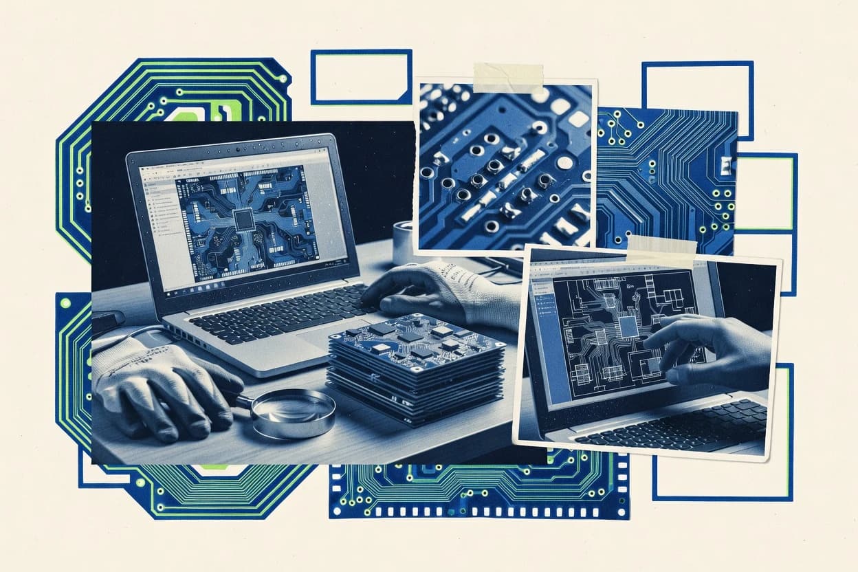
Manufacturing EngineeringTop 10 Best Circut Design Software of 2026
Compare the top 10 Circut Design Software options with a practical ranking. Review Altium Designer, KiCad, and OrCAD picks. Explore now.

How we ranked these tools
Core product claims cross-referenced against official documentation, changelogs, and independent technical reviews.
Analyzed video reviews and hundreds of written evaluations to capture real-world user experiences with each tool.
AI persona simulations modeled how different user types would experience each tool across common use cases and workflows.
Final rankings reviewed and approved by our editorial team with authority to override AI-generated scores based on domain expertise.
Score: Features 40% · Ease 30% · Value 30%
Gitnux may earn a commission through links on this page — this does not influence rankings. Editorial policy
Editor’s top 3 picks
Three quick recommendations before you dive into the full comparison below — each one leads on a different dimension.
Altium Designer
Real-time Design Rule Check with constraint-managed PCB routing and interactive violations
Built for engineering teams building complex PCBs with high constraints and tight documentation control.
KiCad
Design Rule Check with rule sets for nets, clearances, and manufacturing constraints
Built for independent engineers and small teams needing reliable PCB design tooling.
Cadence OrCAD
Constraint-driven PCB routing that enforces design rules across layout revisions
Built for pCB-centric engineering teams needing controlled, repeatable schematic and layout workflows.
Related reading
Comparison Table
This comparison table evaluates circuit design software used for schematic capture, PCB layout, and rules-driven design checks. It contrasts mainstream EDA platforms such as Altium Designer, KiCad, Cadence OrCAD, Mentor Graphics PADS, and Zuken CR-8000 across key areas like workflow fit, tool coverage, and integration paths. Readers can use the results to narrow choices for specific board complexity, collaboration needs, and manufacturing handoff requirements.
| # | Tool | Category | Overall | Features | Ease of Use | Value |
|---|---|---|---|---|---|---|
| 1 | Altium Designer Provides PCB design, schematic capture, and interactive routing with integrated simulation and manufacturing outputs. | professional PCB | 8.9/10 | 9.4/10 | 8.4/10 | 8.8/10 |
| 2 | KiCad Offers open-source schematic capture and PCB layout with Gerber and manufacturing output workflows. | open-source | 8.5/10 | 8.8/10 | 7.8/10 | 8.7/10 |
| 3 | Cadence OrCAD Provides schematic and PCB design tooling with library management and manufacturing-ready export flows. | EDA suite | 7.9/10 | 8.4/10 | 7.6/10 | 7.6/10 |
| 4 | Mentor Graphics PADS Enables schematic and PCB layout workflows optimized for manufacturing output and design reuse. | PCB layout | 7.7/10 | 8.1/10 | 7.2/10 | 7.7/10 |
| 5 | Zuken CR-8000 Delivers schematic and PCB design automation with project data control for industrial electronics manufacturing engineering. | enterprise design | 8.1/10 | 8.8/10 | 7.2/10 | 8.1/10 |
| 6 | Zuken CR-5000 Supports multi-sheet schematic capture and PCB design tasks with rules-based design management for manufacturing. | enterprise PCB | 7.2/10 | 7.8/10 | 6.9/10 | 6.8/10 |
| 7 | Proteus Combines schematic capture and circuit simulation with PCB-related workflows for electronics engineering verification. | simulation-first | 8.1/10 | 8.6/10 | 7.6/10 | 7.8/10 |
| 8 | EasyEDA Provides browser-based schematic capture and PCB layout with online library access and manufacturing file export. | web-based | 8.1/10 | 8.5/10 | 7.8/10 | 7.9/10 |
| 9 | CircuitMaker Supports schematic entry and PCB layout with fabrication output generation for small-to-mid electronics engineering teams. | free tooling | 7.7/10 | 8.0/10 | 7.4/10 | 7.6/10 |
| 10 | RoboDK Generates robotic paths for electronics manufacturing tasks that include printed circuit handling and assembly workflows. | manufacturing automation | 7.0/10 | 7.2/10 | 6.6/10 | 7.1/10 |
Provides PCB design, schematic capture, and interactive routing with integrated simulation and manufacturing outputs.
Offers open-source schematic capture and PCB layout with Gerber and manufacturing output workflows.
Provides schematic and PCB design tooling with library management and manufacturing-ready export flows.
Enables schematic and PCB layout workflows optimized for manufacturing output and design reuse.
Delivers schematic and PCB design automation with project data control for industrial electronics manufacturing engineering.
Supports multi-sheet schematic capture and PCB design tasks with rules-based design management for manufacturing.
Combines schematic capture and circuit simulation with PCB-related workflows for electronics engineering verification.
Provides browser-based schematic capture and PCB layout with online library access and manufacturing file export.
Supports schematic entry and PCB layout with fabrication output generation for small-to-mid electronics engineering teams.
Generates robotic paths for electronics manufacturing tasks that include printed circuit handling and assembly workflows.
Altium Designer
professional PCBProvides PCB design, schematic capture, and interactive routing with integrated simulation and manufacturing outputs.
Real-time Design Rule Check with constraint-managed PCB routing and interactive violations
Altium Designer stands out for deeply integrated schematic, PCB, simulation, and rule-checking workflows in a single editor. The software supports advanced PCB design with real-time design rule checks, constraint-driven routing, and detailed 3D visualization. It also includes strong manufacturing data preparation with customizable outputs like Gerber, drill, and fabrication packages. Projects scale well for complex boards through centralized libraries, versioned components, and collaborative design practices.
Pros
- Real-time design rule checks prevent many layout and constraint mistakes early
- Constraint-driven routing accelerates escape, channel, and high-density layout tasks
- Tightly integrated schematic-to-PCA handoff reduces net and footprint mismatches
- Advanced 3D and visualization supports clear enclosure and mechanical sanity checks
- Robust fabrication output generation supports controlled workflows for complex builds
Cons
- Steep learning curve for rule sets, constraint logic, and advanced routing
- Resource-intensive sessions can slow down large projects on midrange systems
Best For
Engineering teams building complex PCBs with high constraints and tight documentation control
More related reading
KiCad
open-sourceOffers open-source schematic capture and PCB layout with Gerber and manufacturing output workflows.
Design Rule Check with rule sets for nets, clearances, and manufacturing constraints
KiCad stands out for a fully open toolchain that covers schematic capture, PCB layout, and library management in a single environment. It supports a modern workflow with design rule checks, interactive routing tools, and 2D fabrication outputs. Project data can be versioned and reused through libraries, making long-term hardware iteration more practical. Constraint-driven editing and robust DRC help reduce layout mistakes before export.
Pros
- Integrated schematic capture and PCB layout reduces context switching
- Strong design rule checks catch many manufacturability issues early
- Flexible footprints and symbol libraries support repeatable design reuse
- Interactive routing with clear constraint feedback speeds trace planning
Cons
- Complex projects can feel interface-heavy for first-time users
- 3D viewing and simulation are limited compared to specialized ecosystems
- Managing large multi-sheet hierarchies requires careful setup discipline
Best For
Independent engineers and small teams needing reliable PCB design tooling
Cadence OrCAD
EDA suiteProvides schematic and PCB design tooling with library management and manufacturing-ready export flows.
Constraint-driven PCB routing that enforces design rules across layout revisions
Cadence OrCAD stands out with a mature electronics design flow built around schematic capture and PCB layout under a single toolchain. It supports component libraries, netlist-based design reuse, and constraint-driven routing to move from logic to manufacturable boards. The environment is designed for teams that need consistent design data handling across iterations and collaboration. Integration with the broader Cadence design ecosystem strengthens workflows that extend beyond basic schematic and layout tasks.
Pros
- Schematic-to-PCB handoff uses netlists and constraint-driven layout workflows.
- Strong library and design data management supports repeatable revisions.
- Mature routing and constraint features target fabrication-ready board outcomes.
Cons
- UI complexity slows initial setup for small teams and solo users.
- Library customization and rule creation take significant upfront effort.
- Integration benefits are strongest for organizations already using Cadence tools.
Best For
PCB-centric engineering teams needing controlled, repeatable schematic and layout workflows
More related reading
Mentor Graphics PADS
PCB layoutEnables schematic and PCB layout workflows optimized for manufacturing output and design reuse.
Design rule check with configurable constraints across schematics-to-layout verification
Mentor Graphics PADS stands out for its long-used integration between schematic capture and PCB layout workflows in industrial electronics design. It supports standard circuit design tasks like component placement, autorouting, net highlighting, and rule-based design checks using a configurable rules system. Libraries and constraint-driven updates help engineers keep connectivity consistent from schematic through layout without manual reconciliation.
Pros
- Tight schematic-to-PCB connectivity keeps nets consistent during edits
- Rule-based design checks catch clearances, footprints, and constraint violations
- Robust autorouting and interactive routing for dense PCB topologies
- Mature component and footprint library workflows for production design reuse
Cons
- Legacy UI patterns can slow first-time navigation and learning
- Advanced automation requires careful setup of constraints and design rules
- Large projects can feel heavy without disciplined library and data management
Best For
Teams producing production PCBs needing rule-driven checks and mature workflow integration
Zuken CR-8000
enterprise designDelivers schematic and PCB design automation with project data control for industrial electronics manufacturing engineering.
CR-8000 rule-based design checking that enforces schematic and PCB consistency
Zuken CR-8000 is a schematic and PCB design environment built for large, structured electronics development workflows. It emphasizes rule-based data integrity between schematic capture and PCB layout, with controlled object management across design revisions. Teams also get library management and connectivity-aware editing that supports consistent reuse of symbols, footprints, and constraints. The tool is best understood as an engineering workflow system rather than a lightweight editor.
Pros
- Strong schematic-to-layout consistency through connectivity and constraint management
- Robust library handling for symbols, footprints, and design data reuse
- Rule-driven workflows improve large-project data integrity and revision control
Cons
- Interface and command structure feel complex for small, casual design work
- Setup of project standards and rules requires upfront engineering effort
- Workflow tuning can be slow when migrating from different CAD data models
Best For
Engineering teams managing complex PCB projects with strict standards and data control
Zuken CR-5000
enterprise PCBSupports multi-sheet schematic capture and PCB design tasks with rules-based design management for manufacturing.
Rule-based design checking with enforced schematic standards across large projects
Zuken CR-5000 targets professional electrical circuit documentation with a focus on structured schematic design and robust database-driven workflows. The tool supports multi-user project data, rule-based checking, and consistent reuse of components and symbols across large document sets. It also integrates with downstream design activities through established interfaces used in industrial electronics documentation environments. CR-5000 stands out most for managing complex schematic libraries and enforcing design standards across projects.
Pros
- Strong rule-based checking for schematic consistency and design standards
- Good support for large schematic databases and controlled component reuse
- Project-wide data management helps keep references and variants organized
- Facilities for schematic-to-other-electronics workflows through industrial tooling
Cons
- Interface and configuration can feel heavy for smaller projects
- Library setup and governance require disciplined upfront work
- Advanced automation often needs specialized training and process tuning
- Less oriented toward rapid, exploratory schematic drafting
Best For
Industrial electronics teams needing controlled schematic data at scale
More related reading
Proteus
simulation-firstCombines schematic capture and circuit simulation with PCB-related workflows for electronics engineering verification.
Mixed-signal simulation driven by component models within the schematic environment
Proteus stands out for combining schematic capture with simulation in a single workflow built around embedded and microcontroller systems. It supports mixed-signal simulation and broad device modeling so designs can be validated beyond basic logic checks. Tools for PCB layout integrate with the design flow, helping teams move from netlist to board without rebuilding connectivity data. Library management and project organization support multi-sheet schematics and reusable blocks for recurring circuit work.
Pros
- Tight schematic-to-simulation workflow with mixed-signal support
- Strong microcontroller and embedded component modeling for system-level validation
- Integrated PCB layout and connectivity handoff reduces netlist rework
Cons
- Learning curve for advanced simulation setup and model parameters
- Component and behavioral coverage can lag for uncommon niche ICs
- Schematic complexity can become harder to manage in large multi-sheet projects
Best For
Embedded engineers and students validating circuits through simulation and layout
EasyEDA
web-basedProvides browser-based schematic capture and PCB layout with online library access and manufacturing file export.
Unified schematic-to-PCB workflow with integrated PCB rule checks
EasyEDA stands out for combining schematic capture, PCB layout, and fabrication-ready outputs inside one web-first workflow. It includes strong library support with symbol and footprint management, plus PCB rules to help enforce clearances and routing constraints. The platform also supports collaborative sharing through project links and integrates common export formats for downstream tools and manufacturing handoff.
Pros
- Web-based schematic and PCB editor keeps projects accessible across devices
- Library and footprint management streamlines reuse of standard components
- Gerber and drill outputs support common manufacturing handoffs
Cons
- Complex designs can feel slower than desktop-first CAD workflows
- Advanced constraint control requires more setup than simpler tools
- Exported results can need extra verification for tight production specs
Best For
Engineers needing browser-based PCB design with reliable fabrication exports
More related reading
CircuitMaker
free toolingSupports schematic entry and PCB layout with fabrication output generation for small-to-mid electronics engineering teams.
Rule-based ERC and DRC checks in the design flow
CircuitMaker focuses on creating and sharing PCB designs with a workflow built around schematic capture and a dedicated PCB layout editor. The software supports symbol and footprint creation plus rule-driven design checks to catch common electrical and manufacturing issues. Library management and project organization enable teams to reuse parts across multiple boards without rebuilding footprints from scratch.
Pros
- Tight schematic-to-PCB workflow reduces sync errors
- Built-in design rule checks catch routing and clearance issues early
- Reusable part libraries speed creation of consistent PCB footprints
Cons
- Advanced routing and constraints take time to learn
- Simulation and complex verification are limited versus full EDA suites
- Large multi-sheet designs can feel slower in heavy libraries
Best For
Small to mid-size teams designing PCBs that need repeatable libraries
RoboDK
manufacturing automationGenerates robotic paths for electronics manufacturing tasks that include printed circuit handling and assembly workflows.
Collision detection during robotic path simulation with CAD scene integration
RoboDK stands out by combining robot simulation with offline programming workflows inside a single toolchain. It supports CAD import, robot path planning, and collision-aware cycle verification for industrial automation tasks. For circuit design work, it can help visualize toolpaths for PCB routing or placement processes when robot kinematics are involved. It does not provide a dedicated electronic CAD environment like schematic capture and PCB layout editors.
Pros
- Collision checking and offline programming for automated PCB tooling workflows
- Robot kinematics simulation that helps validate cell behavior before execution
- CAD and mesh import that supports custom fixtures and hardware visualization
Cons
- Not a schematic capture and PCB layout tool for circuit design deliverables
- Setup time is higher when configuring robots, workspaces, and reference frames
- Toolpath generation depends on external CAD/CAM or manual path creation
Best For
Teams simulating robot-assisted PCB processing and verifying collision-safe tooling
How to Choose the Right Circut Design Software
This buyer’s guide explains how to choose circuit design software for schematic capture, PCB layout, and manufacturing handoff. It covers tools including Altium Designer, KiCad, Proteus, EasyEDA, and RoboDK, along with enterprise-focused options like Cadence OrCAD and Mentor Graphics PADS. It also clarifies where simulation and rule checking fit into the decision so electronics teams can pick the right workflow for their deliverables.
What Is Circut Design Software?
Circut design software covers the workflows used to create electronics schematics and translate them into manufacturable PCB layouts. It typically includes design rule checks for nets and clearances, constraint-driven routing, and fabrication export generation such as Gerber and drill outputs. Some tools also combine schematic capture with circuit simulation, including Proteus for mixed-signal validation. Others focus on browser-first PCB work, including EasyEDA, or industrial engineering document control, including Zuken CR-8000 and Zuken CR-5000.
Key Features to Look For
These capabilities determine how reliably a schematic turns into a correct PCB layout and whether a team can validate behavior before manufacturing.
Real-time design rule checks with interactive violations
Altium Designer provides real-time design rule checks that surface constraint violations during routing, which helps prevent many layout and constraint mistakes early. KiCad also delivers design rule checks with rule sets for nets, clearances, and manufacturing constraints. EasyEDA includes integrated PCB rule checks inside its unified schematic-to-PCB workflow.
Constraint-driven routing for high-density escapes and controlled layouts
Altium Designer uses constraint-managed PCB routing that accelerates escape and high-density layout tasks. Cadence OrCAD focuses on constraint-driven PCB routing that enforces design rules across layout revisions, which supports consistent fabrication outcomes. Mentor Graphics PADS provides robust autorouting and interactive routing for dense PCB topologies with rule-based checks.
Tight schematic-to-PCB connectivity and handoff
Altium Designer emphasizes tightly integrated schematic-to-PCB handoff to reduce net and footprint mismatches. Mentor Graphics PADS maintains schematic-to-PCB connectivity so nets stay consistent during edits and verification. CircuitMaker also uses a tight schematic-to-PCB workflow to reduce sync errors and keep part libraries aligned.
Manufacturing output generation and fabrication-ready export workflows
Altium Designer offers robust fabrication output generation with customizable fabrication packages that support complex builds. KiCad supports Gerber and manufacturing output workflows for boards that need standardized export deliverables. EasyEDA outputs Gerber and drill files for common manufacturing handoffs.
Library and rule governance for repeatable revisions
Altium Designer supports centralized libraries, versioned components, and collaborative practices that help complex projects scale. Zuken CR-8000 provides rule-driven workflows and controlled object management that enforces schematic and PCB consistency across revisions. Zuken CR-5000 focuses on multi-user project data and database-driven workflows that enforce design standards across large schematic sets.
Built-in simulation for schematic-level verification
Proteus combines schematic capture with mixed-signal simulation driven by component models, which supports circuit validation beyond basic logic checks. This mixed-signal simulation workflow reduces the need to rebuild connectivity data when moving toward PCB-related verification. Other tools in the set focus primarily on schematic and PCB design deliverables rather than embedded circuit simulation.
How to Choose the Right Circut Design Software
Choosing the right tool depends on how much rule enforcement, simulation, and data governance the deliverable requires.
Match the workflow to the deliverable
If the deliverable is a complex PCB with stringent constraints and documentation discipline, Altium Designer is built around deeply integrated schematic, PCB, simulation, and rule-checking workflows. If the main goal is a reliable open-source schematic-to-PCB toolchain with DRC support, KiCad fits teams that need rule sets and export workflows without relying on a proprietary ecosystem. If the deliverable includes circuit validation before layout, Proteus combines schematic capture with mixed-signal simulation so behavioral issues can be found early.
Prioritize rule checking where mistakes are most expensive
For teams that need violations surfaced during routing, Altium Designer provides real-time design rule checks with interactive constraint-managed routing. Cadence OrCAD enforces design rules across layout revisions using constraint-driven routing, which reduces regression risk between iterations. Mentor Graphics PADS and KiCad also rely on configurable or rule-set-driven design checks that catch clearances and manufacturability issues before export.
Evaluate connectivity integrity from schematic to layout
Altium Designer and Mentor Graphics PADS both emphasize keeping nets consistent during schematic-to-layout edits, which helps prevent net and footprint mismatches. CircuitMaker also targets reduced sync errors through a tight schematic-to-PCB workflow and rule-driven checks. For industrial teams running large documentation structures, Zuken CR-8000 and Zuken CR-5000 emphasize connectivity-aware editing and controlled object management to preserve schematic and PCB consistency.
Confirm manufacturing export readiness for the boards being built
Altium Designer supports detailed fabrication output generation such as Gerber, drill, and fabrication packages that suit complex controlled builds. KiCad supports Gerber and manufacturing output workflows, and its DRC help reduces manufacturability issues before export. EasyEDA integrates Gerber and drill outputs into a browser-based schematic and PCB workflow for fabrication handoff.
Choose the right environment for your scale and collaboration needs
Desktop-first, engineering-heavy workflows often favor Altium Designer, Cadence OrCAD, and Mentor Graphics PADS due to their complex routing and rule systems. Browser-first collaboration often favors EasyEDA because it keeps the schematic and PCB design workflow accessible across devices and includes project link sharing. If robot-assisted PCB processing verification is part of the workflow, RoboDK is the automation-oriented option because it focuses on collision detection and offline robot path simulation and does not replace schematic capture and PCB layout.
Who Needs Circut Design Software?
Different teams need different balances of schematic capture, PCB layout, rule enforcement, simulation, and manufacturing handoff.
Engineering teams building complex PCBs with high constraints and tight documentation control
Altium Designer is a strong fit for this audience because it provides real-time design rule checks, constraint-managed PCB routing, and tightly integrated schematic-to-PCBA handoff with advanced 3D visualization. Cadence OrCAD also fits teams needing constraint-driven routing and repeatable schematic and layout workflows under a mature rule-based flow.
Independent engineers and small teams that need dependable PCB design tooling with strong DRC
KiCad suits this segment because it combines schematic capture and PCB layout in a single open toolchain with DRC rule sets for nets, clearances, and manufacturing constraints. CircuitMaker also targets small to mid-size teams that need repeatable libraries and rule-based ERC and DRC checks in the design flow.
Embedded engineers and students validating circuits using simulation-driven verification
Proteus fits this group because it combines schematic capture with mixed-signal simulation driven by component models and supports system-level validation for microcontroller designs. The integrated schematic-to-simulation workflow helps reduce netlist rework when transitioning toward PCB-related verification.
Industrial electronics teams that manage large schematic databases and enforce standards across projects
Zuken CR-8000 fits engineering teams that need rule-based schematic and PCB consistency plus controlled object management across revisions for structured manufacturing engineering workflows. Zuken CR-5000 targets controlled schematic data at scale with rule-based checking across large multi-sheet document sets and enforced schematic standards.
Common Mistakes to Avoid
Selection pitfalls across these tools usually come from mismatched workflow depth, inadequate rule governance, or assuming an automation tool can replace electronics design deliverables.
Expecting a robot simulation tool to replace PCB design deliverables
RoboDK is collision detection and offline robot path simulation software integrated with CAD scene work, so it does not provide dedicated schematic capture and PCB layout deliverables. Teams needing schematics, PCB routing, and design rule checks should choose tools like Altium Designer, KiCad, EasyEDA, or CircuitMaker instead of RoboDK.
Underestimating setup effort for complex rule and library governance
Altium Designer, Cadence OrCAD, and Mentor Graphics PADS can require steep learning for advanced rule sets and constraint logic, so teams should plan time for rule configuration. Zuken CR-8000 and Zuken CR-5000 also require upfront engineering effort to set project standards and rule workflows for controlled schematic-to-layout data integrity.
Skipping validation steps before export and manufacturing handoff
Ignoring design rule checks can let clearance and constraint issues reach export, which is exactly what the built-in DRC systems in KiCad, EasyEDA, and CircuitMaker are designed to prevent. Altium Designer and Cadence OrCAD help avoid late-stage errors by enforcing constraint-driven routing and surfacing interactive violations while the layout is being built.
Choosing a tool that cannot support the scale of schematic documentation
Complex projects can feel interface-heavy in KiCad and heavy in Mentor Graphics PADS when multi-sheet hierarchies are not governed carefully. Zuken CR-5000 and Zuken CR-8000 are built for large schematic databases and controlled standards, which makes them better fits when governance and scale are primary requirements.
How We Selected and Ranked These Tools
we evaluated each tool on three sub-dimensions with these weights: features at 0.4, ease of use at 0.3, and value at 0.3. The overall rating for each tool is the weighted average of those three sub-dimensions using overall = 0.40 × features + 0.30 × ease of use + 0.30 × value. Altium Designer separated itself by combining features depth with strong manufacturing and rule-enforcement capability, including real-time design rule checks and tightly integrated schematic-to-PCBA workflows that reduce routing and documentation mistakes while maintaining controlled fabrication output generation.
Frequently Asked Questions About Circut Design Software
Which circuit design tool is strongest for constraint-driven PCB routing with real-time rule checking?
Altium Designer provides real-time Design Rule Check tied to constraint-managed PCB routing, with interactive violation highlighting during layout. KiCad also offers a DRC workflow with rule sets for nets, clearances, and manufacturing constraints, but Altium centers the workflow in a deeply integrated editor.
What’s the best option for teams that need one integrated workflow from schematic to manufacturing outputs?
Altium Designer connects schematic capture, PCB design, and manufacturing data preparation inside one editor, including customizable outputs like Gerber and drill packages. EasyEDA also unifies schematic-to-PCB work in a single web-first flow with fabrication-ready exports, with integrated PCB rule checks for clearance and routing constraints.
Which tools fit simulation-heavy circuit validation instead of only schematic and PCB design?
Proteus combines schematic capture with mixed-signal simulation driven by component models, which supports validation beyond net connectivity. RoboDK can add a simulation-driven layer for robot-assisted PCB processing by using CAD import, collision-aware cycle verification, and toolpath planning, even though it is not an electronic CAD environment.
How do open-toolchain workflows compare between KiCad and proprietary editors like Altium Designer?
KiCad uses an open toolchain that covers schematic capture, PCB layout, and library management in one environment, which helps keep project data reusable across long-term iteration. Altium Designer is proprietary and focuses on deeply integrated rule checking, constraint-managed routing, and centralized library workflows for complex boards.
Which circuit design software is best for industrial schematic documentation and large multi-document projects?
Zuken CR-5000 targets professional electrical circuit documentation with database-driven, multi-user workflows and rule-based checking across large document sets. Zuken CR-8000 emphasizes structured engineering workflows with controlled object management and rule-based data integrity between schematic capture and PCB layout.
Which tool is most appropriate when schematic-to-layout connectivity must stay consistent without manual reconciliation?
Mentor Graphics PADS uses libraries and rule-based design checks with configurable constraints to keep connectivity consistent from schematic through layout. Zuken CR-8000 and Zuken CR-5000 both add rule-based integrity enforcement across design revisions by managing objects with connectivity-aware editing.
What should be selected for embedded systems teams that need simulation and then board work in the same workflow?
Proteus fits embedded engineering because it combines schematic capture and simulation for microcontroller and mixed-signal verification in one workflow. EasyEDA fits teams that prioritize browser-based schematic and PCB work with fabrication-ready outputs, while Proteus emphasizes validation through simulation-driven models.
Which tools support collaborative or sharing workflows for multi-user or link-based project access?
EasyEDA supports collaborative sharing through project links while keeping schematic capture and PCB layout in a unified web-first workflow. Cadence OrCAD is built for teams needing consistent design data handling across iterations and collaboration, especially when the broader Cadence design ecosystem is used.
What’s a common technical pitfall when switching circuit design tools, and which software helps reduce it?
Connectivity and footprint mismatches often appear during tool migration, but KiCad’s integrated DRC plus library management helps catch layout mistakes before export. Altium Designer reduces routing and rule violations with real-time DRC tied to constraint-managed routing, which lowers the chance that schematic assumptions diverge from board reality.
Conclusion
After evaluating 10 manufacturing engineering, Altium Designer stands out as our overall top pick — it scored highest across our combined criteria of features, ease of use, and value, which is why it sits at #1 in the rankings above.
Use the comparison table and detailed reviews above to validate the fit against your own requirements before committing to a tool.
Tools reviewed
Referenced in the comparison table and product reviews above.
Keep exploring
Comparing two specific tools?
Software Alternatives
See head-to-head software comparisons with feature breakdowns, pricing, and our recommendation for each use case.
Explore software alternatives→In this category
Manufacturing Engineering alternatives
See side-by-side comparisons of manufacturing engineering tools and pick the right one for your stack.
Compare manufacturing engineering tools→FOR SOFTWARE VENDORS
Not on this list? Let’s fix that.
Our best-of pages are how many teams discover and compare tools in this space. If you think your product belongs in this lineup, we’d like to hear from you—we’ll walk you through fit and what an editorial entry looks like.
Apply for a ListingWHAT THIS INCLUDES
Where buyers compare
Readers come to these pages to shortlist software—your product shows up in that moment, not in a random sidebar.
Editorial write-up
We describe your product in our own words and check the facts before anything goes live.
On-page brand presence
You appear in the roundup the same way as other tools we cover: name, positioning, and a clear next step for readers who want to learn more.
Kept up to date
We refresh lists on a regular rhythm so the category page stays useful as products and pricing change.