GITNUXSOFTWARE ADVICE
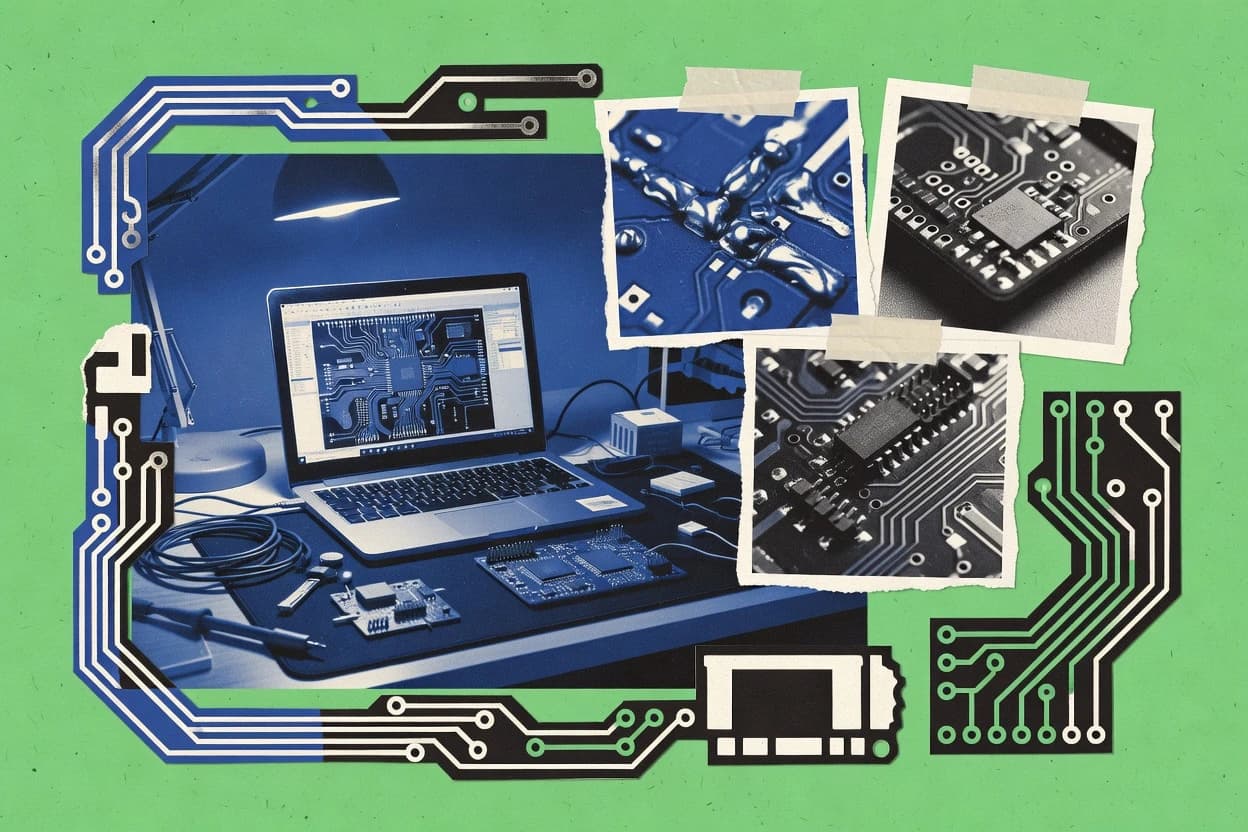
Manufacturing EngineeringTop 10 Best Circuits Design Software of 2026
Top 10 Circuits Design Software for 2026. Compare Altium, Fusion 360, OrCAD, and more to find the best fit for circuit design.

How we ranked these tools
Core product claims cross-referenced against official documentation, changelogs, and independent technical reviews.
Analyzed video reviews and hundreds of written evaluations to capture real-world user experiences with each tool.
AI persona simulations modeled how different user types would experience each tool across common use cases and workflows.
Final rankings reviewed and approved by our editorial team with authority to override AI-generated scores based on domain expertise.
Score: Features 40% · Ease 30% · Value 30%
Gitnux may earn a commission through links on this page — this does not influence rankings. Editorial policy
Editor’s top 3 picks
Three quick recommendations before you dive into the full comparison below — each one leads on a different dimension.
Altium Designer
Constraint-driven design engine that enforces schematic-to-PCB rules across the layout
Built for teams designing complex, high-density PCBs needing strict rules and automation.
Autodesk Fusion 360 Electronics
Editor pick3D co-design with Fusion 360 for electronics-to-mechanics assembly alignment
Built for teams needing PCB layout plus 3D mechanical co-design in one workflow.
Cadence OrCAD/Allegro
Editor pickAllegro Constraint Manager for rule-driven design intent enforcement during placement and routing
Built for high-speed PCB teams needing constraint-driven routing, verification, and tight workflow control.
Related reading
Comparison Table
This comparison table maps key capabilities across circuits and PCB design software, including Altium Designer, Autodesk Fusion 360 Electronics, Cadence OrCAD and Allegro, Siemens EDA tools, KiCad, and additional alternatives. Readers can compare design workflows, schematic and PCB features, simulation and verification support, component and library management, and integration with manufacturing outputs to shortlist tools that match specific project requirements.
Altium Designer
pcb design suitePerforms schematic capture, PCB layout, and manufacturing-ready outputs for printed circuit boards in a single integrated design environment.
Constraint-driven design engine that enforces schematic-to-PCB rules across the layout
Altium Designer stands out for tightly integrated schematic, PCB, and managed rule-driven design workflows that stay consistent across the toolchain. The platform combines powerful constraint management, signal and power integrity analysis, and robust routing and manufacturing outputs.
Library management and collaboration features support multi-user projects, including reusable design data and version-controlled components. The result is a circuit design environment optimized for complex boards rather than quick single-board sketches.
- +End-to-end schematic to PCB flows with consistent rule enforcement
- +Advanced constraint and interactive routing for high-density layouts
- +Strong DRC and manufacturing output generation for fabrication readiness
- +Feature-rich library management with reusable, component-safe workflows
- +Integrated simulation and analysis tools for electrical validation
- –Tooling depth creates a steep learning curve for new users
- –Large projects can feel heavy in responsiveness without tuning
- –Some workflows require careful setup of rules and templates
- –Deep configuration options can slow early iteration cycles
Best for: Teams designing complex, high-density PCBs needing strict rules and automation
More related reading
Autodesk Fusion 360 Electronics
electronics CADCreates PCB designs with integrated schematic capture and electronics design workflows inside the Fusion electronics environment.
3D co-design with Fusion 360 for electronics-to-mechanics assembly alignment
Autodesk Fusion 360 Electronics stands out by merging circuit design with parametric 3D CAD workflows so layout and mechanical context share the same data model. It covers schematic capture, PCB layout, and rules-based design checks, with a workflow built around electronics-to-3D assembly iteration.
The tool also supports electronics documentation outputs and integrates with simulation and manufacturing handoff steps typical of professional PCB work. For complex boards, it emphasizes constraint-driven placement and trace routing tied to board stack and component models.
- +Tight link between PCB editing and Fusion 3D mechanical context
- +Rules-based design checks catch clearance and footprint issues
- +Constraint-driven PCB workflow improves repeatability on complex boards
- +Schematic-to-board data reduces manual synchronization errors
- –Electronics-centric setup can feel heavy for small quick-turn boards
- –Advanced routing and stack configuration takes time to master
- –Mixed workflows require careful library and model hygiene
Best for: Teams needing PCB layout plus 3D mechanical co-design in one workflow
Cadence OrCAD/Allegro
enterprise pcbSupports circuit board schematic entry and constraint-driven PCB layout with manufacturing and verification flows for professional electronics engineering.
Allegro Constraint Manager for rule-driven design intent enforcement during placement and routing
Cadence OrCAD and Allegro deliver a tightly integrated schematic-to-PCB workflow focused on high signal-integrity and manufacturing-ready layouts. Allegro excels at advanced PCB design with robust constraint handling, detailed routing capabilities, and power and grounding tooling.
OrCAD captures and organizes schematics with library management and simulation-friendly netlist flows into downstream implementation. Together, the suite supports large, complex boards and real-world verification loops across multiple design stages.
- +Allegro routing and constraint management handle dense, high-speed boards reliably
- +Tight schematic-to-layout workflow supports consistent netlists and design intent transfer
- +Strong DRC and manufacturing-oriented checks reduce late-stage layout surprises
- –Workflow depth creates a steep learning curve for first-time layout engineers
- –Tool configuration and libraries require setup time to match team design standards
- –Performance tuning for very large projects can be nontrivial
Best for: High-speed PCB teams needing constraint-driven routing, verification, and tight workflow control
More related reading
Siemens EDA (Altium alternatives in Siemens portfolio)
enterprise EDAEnables schematic and PCB design workflows with electronic design automation capabilities aimed at manufacturing-grade electronics development.
Constraint-driven design management across schematic-to-layout with automated rule enforcement
Siemens EDA stands out by aligning PCB and schematic workflows with Siemens design governance for large, regulated engineering organizations. Core capabilities include schematic capture, PCB layout, constraint-driven design, and manufacturing data preparation via standard CAD outputs.
Typical workflows span from design entry and routing to DFM-focused checks and handoff packages for fabrication. The suite targets system-scale collaboration rather than single-designer hobby use.
- +Constraint-driven PCB design supports repeatable electrical and physical rules
- +Strong manufacturing handoff coverage for fabrication and assembly data packages
- +Works well in team environments needing controlled design processes
- –Workflow setup can be heavy for organizations without established standards
- –Advanced features require training to use effectively for complex rule sets
- –Tooling integration can feel complex when mixing with nonstandard toolchains
Best for: Mid-to-large teams needing governed PCB design workflows and reliable manufacturing handoff
KiCad
open-sourceProvides open-source schematic capture and PCB layout tooling with Gerber and drill file export for fabrication.
Single unified KiCad project linking schematic netlists to PCB layout connectivity
KiCad stands out for running the full schematic to PCB workflow in a single open source toolchain, including both layout and electronics symbol management. The core capabilities include schematic capture, ERC, PCB layout with DRC and net connectivity checks, and a unified library system for footprints and symbols. KiCad also provides 3D visualization for PCB assemblies through its built-in viewer to validate mechanical fit alongside electrical design.
- +Integrated schematic capture, PCB layout, and validation checks in one application
- +Powerful footprint and symbol libraries with clear separation between components and packages
- +Strong DRC and net connectivity workflows to catch layout issues before export
- +3D viewer supports mechanical sanity checks for footprints and board keepouts
- +Automation via scripting and reusable project files reduces repetitive design work
- –Complex projects can feel slower to navigate than more commercial CAD workflows
- –Learning advanced features like constraint management takes noticeable training time
- –Some third-party workflows rely on add-ons or export formats for seamless integration
- –Design rule customization offers depth but requires careful setup to avoid false positives
Best for: Engineers and makers needing full PCB design control without proprietary lock-in
EPLAN
industrial electricalCreates electrical engineering schematics and project documentation with data structures that support downstream manufacturing and system integration.
EPLAN’s Layout and Wiring logic with rules-based automation for consistent electrical documentation
EPLAN stands out for engineering-centric automation in electrical and circuit documentation workflows. It supports schematic capture, routing-oriented wiring logic, and rules-driven consistency checks that reduce rework across large projects.
The system also integrates with a broader EPLAN environment for parts data, revision handling, and structured documentation outputs. Strong cross-referencing features help maintain traceability from schematic logic through labeling and documentation sets.
- +Strong rule-based consistency checks for schematics and documentation sets
- +Robust part and terminal data management with traceable naming and references
- +Automation options for cable and wiring logic aligned with engineering practices
- +Configurable report and publication outputs for structured documentation packages
- –Setup of naming, rules, and templates can take significant initial configuration
- –User experience feels specialized for electrical documentation rather than CAD-only drafting
- –Learning curve is steep for advanced automation and project data workflows
Best for: Electrical engineering teams needing rule-driven circuit documentation automation at scale
More related reading
Mentor PADS (part of Siemens EDA)
pcb layoutDelivers schematic entry and PCB layout tooling with design rule checks and fabrication output for printed circuit boards.
Technology file and rules framework powering DRC, constraints, and design consistency across boards
Mentor PADS stands out for its complete PCB design workflow that combines schematic capture, PCB layout, and signal integrity checks in a single Siemens EDA toolset. It supports technology files, reusable component libraries, and constraints-driven design to keep large designs consistent across teams.
Automated routing, placement assistance, and DRC style checking help reduce manual iteration during layout. For higher-end verification and manufacturing handoff, it typically integrates with the broader Siemens EDA ecosystem rather than replacing every specialist tool.
- +Strong PCB layout toolkit with constraint-driven placement and routing
- +Reliable DRC coverage with techfile-based rule management
- +Good integration paths into Siemens EDA verification workflows
- –Setup of techfiles and rule sets can require experienced admin support
- –User experience can feel complex on large, multi-constraint projects
- –Advanced SI and verification depth depends on connected specialist tools
Best for: Teams needing constraint-based PCB design with automated routing and robust rule checking
Proteus Design Suite
simulate-and-designSupports schematic capture and PCB visualization with simulation and verification workflows used for electronics prototyping and test.
Virtual instrument-driven circuit testing inside the Proteus simulation environment
Proteus Design Suite stands out for tying circuit simulation directly to schematic capture and PCB-oriented workflows. The suite supports schematic-driven simulation and debugging, including mixed-signal models and instrument-based virtual testing. It is well suited to lab-style verification where designers probe signals, step through behavior, and iterate on electronics quickly.
- +Schematic-driven mixed-signal simulation with interactive probing
- +Virtual instruments enable lab-style validation without bench hardware
- +Strong component library coverage for electronics prototyping workflows
- +Co-simulation workflows support practical verification of digital and analog designs
- –Learning curve for simulation setup and model alignment
- –Simulation performance can suffer on large mixed-signal schematics
- –Complex design flows require careful project organization to avoid errors
- –Some advanced analysis options feel less streamlined than specialized tools
Best for: Teams validating mixed-signal electronics through schematic simulation and virtual instrumentation
More related reading
OrCAD Capture and PCB Editor (legacy brand within Cadence portfolio)
cadence captureCreates schematics and PCB layouts with library and manufacturing output flows used in electronics design projects.
Capture’s connectivity and electrical rule checking that drives layout correctness in PCB Editor
OrCAD Capture and PCB Editor stand out for tight schematic-to-layout alignment inside the OrCAD flow. Capture supports component libraries, hierarchical schematics, net connectivity checking, and electrical rule checking to reduce integration errors.
PCB Editor provides board-level design with constraint-driven placement, autorouting options, and shape and manufacturing layers for producing fabrication-ready layouts. The package targets established workflows in legacy Cadence-centric environments and can feel less streamlined than newer unified design toolsets.
- +Strong schematic-to-PCB connectivity with net consistency checking in Capture
- +Mature PCB layout toolset with constraints, routing control, and board shapes
- +Good EDA workflow fit for teams already using Cadence design conventions
- –Legacy UI patterns can slow editing for new teams and faster iteration cycles
- –Modern design-data workflows are less unified than newer EDA suites
- –Cross-tool automation requires more manual setup than integrated alternatives
Best for: Teams maintaining legacy Cadence flows for schematic capture and PCB layout
Spider Software (Circuitboard manufacturing documentation tooling)
manufacturing dataGenerates and manages manufacturing documentation and job data flows connected to circuit board production processes.
Automated manufacturing documentation output generation tied to PCB revisions and deliverable structure
Spider Software centers on manufacturing documentation for circuit board production, with workflows built around generating PCB outputs and keeping them consistent across revisions. The tool focuses on documentation automation rather than schematic capture or PCB layout, so its core value appears in deliverable generation, checklists, and output packaging.
Teams using it for production-ready documentation typically benefit from reduced manual formatting and fewer transcription errors. Documentation can be structured around board variants and manufacturing requirements to streamline repeat jobs from the same design baseline.
- +Strong manufacturing-document automation for PCB deliverables and output packaging
- +Revision-aware documentation generation reduces manual formatting drift
- +Structured outputs support repeatable production documentation workflows
- –Limited scope outside documentation creation for circuit design processes
- –Workflow setup can be time-consuming for teams new to the tool
- –Less suited for interactive design work compared with full EDA suites
Best for: Teams needing automated, revision-controlled PCB manufacturing documentation generation
How to Choose the Right Circuits Design Software
This buyer’s guide helps select circuits design software for schematic capture, PCB layout, verification, and manufacturing deliverables. It covers Altium Designer, Autodesk Fusion 360 Electronics, Cadence OrCAD/Allegro, Siemens EDA, KiCad, EPLAN, Mentor PADS, Proteus Design Suite, OrCAD Capture and PCB Editor, and Spider Software. The guidance focuses on concrete tool capabilities like constraint-driven design, rule enforcement, 3D co-design, mixed-signal simulation, and revision-aware manufacturing documentation.
What Is Circuits Design Software?
Circuits design software is the set of applications used to create electronic designs starting from schematic capture and continuing through PCB layout and fabrication-ready outputs. These tools manage design intent like connectivity, footprints, and routing constraints while running checks such as DRC and electrical rule checking. Many tools also support verification loops through simulation and offer structured output generation for fabrication packages and documentation. Altium Designer and Autodesk Fusion 360 Electronics show what this looks like in practice by combining schematic-to-PCB workflows with design-rule enforcement and, for Fusion 360 Electronics, electronics-to-3D assembly context.
Key Features to Look For
The highest-performing tool matches the feature set to the real work done on a project, from rule enforcement and constraints to simulation and manufacturing documentation.
Constraint-driven schematic-to-PCB rule enforcement
Constraint-driven design management is the core differentiator for enforcing schematic-to-PCB rules during placement and routing. Altium Designer uses a constraint-driven design engine that enforces schematic-to-PCB rules across the layout, and Cadence OrCAD/Allegro adds Allegro Constraint Manager for rule-driven design intent enforcement during placement and routing.
Unified connectivity workflow linking schematic netlists to PCB layout
A unified netlist-to-layout workflow reduces integration errors by keeping electrical intent consistent during edits. KiCad runs a single open source toolchain where schematic netlists link directly to PCB layout connectivity, and OrCAD Capture and PCB Editor provides tight schematic-to-layout alignment inside the OrCAD flow with net connectivity checking.
Advanced DRC and manufacturing-oriented checks that reduce late-stage surprises
DRC and manufacturing-oriented checks catch physical and electrical issues before fabrication handoff. Altium Designer emphasizes strong DRC and manufacturing output generation for fabrication readiness, and Cadence OrCAD/Allegro focuses on strong DRC and manufacturing-oriented checks for reducing late-stage layout surprises.
Integrated library management for symbols and footprints with reusable, safe workflows
Reliable symbol and footprint libraries prevent rework caused by component mismatches across teams. Altium Designer provides feature-rich library management with reusable, component-safe workflows, and KiCad provides powerful footprint and symbol libraries with clear separation between components and packages.
Electronics-to-mechanics 3D co-design context
3D co-design helps ensure connectors, board keepouts, and mechanical constraints align with the PCB layout. Autodesk Fusion 360 Electronics ties PCB editing to Fusion 3D mechanical context for electronics-to-mechanics assembly alignment, and KiCad includes built-in 3D visualization for mechanical sanity checks alongside electrical design.
Mixed-signal simulation with virtual instrument-driven testing
Simulation that starts from schematics and supports interactive testing speeds up validation before board spins. Proteus Design Suite supports schematic-driven mixed-signal simulation with interactive probing and virtual instrument-driven circuit testing inside the Proteus simulation environment.
How to Choose the Right Circuits Design Software
The right choice follows a simple sequence: pick the design workflow fit first, then match verification and output requirements, then confirm team governance and integration needs.
Choose the design workflow model that matches the real project work
For complex, high-density PCB work needing strict rules and automation, Altium Designer is built around end-to-end schematic capture and PCB layout with consistent rule enforcement. For teams that must keep electronics and 3D mechanical context synchronized, Autodesk Fusion 360 Electronics ties PCB editing to Fusion 3D assembly alignment and supports rules-based design checks.
Validate how rule enforcement works during placement and routing
High-speed and dense board teams should prioritize constraint-driven rule enforcement during placement and routing using Cadence OrCAD/Allegro with Allegro Constraint Manager. Large governed environments should evaluate Siemens EDA or Mentor PADS because both emphasize technology file and rules frameworks that power DRC, constraints, and design consistency across boards.
Confirm the connectivity backbone and schematic-to-layout integrity checks
KiCad’s single unified project linking schematic netlists to PCB layout connectivity supports consistent electrical intent during edits. OrCAD Capture and PCB Editor focuses on Capture connectivity with electrical rule checking that drives layout correctness in PCB Editor, which suits teams maintaining legacy Cadence-centric workflows.
Match verification to the electronics domain and iteration style
If the project requires mixed-signal validation with instrument-like debugging, Proteus Design Suite offers schematic-driven mixed-signal simulation plus virtual instruments for lab-style validation without bench hardware. If the goal is primarily DRC and manufacturing-ready layout quality, Altium Designer and Cadence OrCAD/Allegro concentrate verification on rule enforcement and fabrication-oriented outputs.
Plan manufacturing documentation and handoff deliverables up front
When the delivery pipeline is documentation-heavy and revision-controlled, Spider Software focuses on automated manufacturing documentation output generation tied to PCB revisions and deliverable structure. When the deliverables are electrical engineering schematics and traceable documentation sets, EPLAN emphasizes rule-driven consistency checks plus configurable report and publication outputs for structured documentation packages.
Who Needs Circuits Design Software?
Circuits design software benefits teams that must turn electronic intent into manufacturable PCB designs and supporting validation or documentation deliverables.
Teams designing complex, high-density PCBs with strict rule needs
Altium Designer suits this audience because it enforces schematic-to-PCB constraints across layout and emphasizes strong DRC and manufacturing output generation. Cadence OrCAD/Allegro also fits because Allegro Constraint Manager supports rule-driven placement and routing for dense, high-speed boards.
Teams combining PCB design with mechanical co-design
Autodesk Fusion 360 Electronics targets this work by using 3D co-design with Fusion 360 for electronics-to-mechanics assembly alignment. KiCad supports the same intent at the PCB level through built-in 3D visualization for mechanical sanity checks alongside electrical design.
Mid-to-large organizations that need governed PCB design workflows and controlled handoff
Siemens EDA targets system-scale collaboration with constraint-driven design management and automated rule enforcement across schematic-to-layout. Mentor PADS complements this by using technology files and rules frameworks for DRC, constraints, and design consistency across boards.
Electrical documentation teams that automate schematic consistency and labeling at scale
EPLAN is built for engineering-centric automation in electrical and circuit documentation workflows with rules-based consistency checks and robust part and terminal data management. This helps teams maintain traceability from schematic logic through labeling and structured documentation sets.
Common Mistakes to Avoid
Common failure modes show up across tools as either rule setup overhead, workflow mismatch, or missing documentation automation for production.
Underestimating rule and constraint setup work for advanced toolchains
Altium Designer and Cadence OrCAD/Allegro both include deep configuration and rule-based workflows that can slow early iteration if rules and templates are not set up deliberately. Siemens EDA and Mentor PADS also rely on technology files and rule sets that require experienced admin support to match team design standards.
Choosing a simulation-first tool for manufacturing-centric PCB layout control
Proteus Design Suite excels at schematic-driven mixed-signal simulation and virtual instrument testing, but it is not positioned as an end-to-end PCB manufacturing layout control system. Spider Software focuses on manufacturing documentation automation rather than interactive schematic capture and PCB layout.
Assuming legacy UI patterns and workflows will accelerate edits in modern teams
OrCAD Capture and PCB Editor can feel less streamlined due to legacy UI patterns that slow editing for new teams and slower iteration cycles. For teams seeking more unified workflows, KiCad and Altium Designer provide integrated schematic-to-PCB experiences inside a single toolchain.
Not planning for version-controlled deliverables and revision-aware documentation
Spider Software is designed around revision-aware documentation generation tied to PCB deliverable structures, which prevents documentation drift across production runs. Teams that skip this need to automation-focused deliverable packaging often end up doing manual formatting and checklist work outside the design tool.
How We Selected and Ranked These Tools
We evaluated every tool on three sub-dimensions. Features carry a weight of 0.4, ease of use carries a weight of 0.3, and value carries a weight of 0.3. The overall rating is the weighted average computed as overall = 0.40 × features + 0.30 × ease of use + 0.30 × value. Altium Designer separated itself from lower-ranked tools by pairing high feature depth with strong ease-to-use for end-to-end flows, demonstrated by its constraint-driven design engine that enforces schematic-to-PCB rules across the layout.
Frequently Asked Questions About Circuits Design Software
Which circuits design software keeps schematic rules consistent during PCB layout on complex boards?
What tool is best when PCB design must share a single data model with 3D mechanical context?
Which suite is designed for high-speed signal integrity work with verification loops tied to layout?
What software supports governed, regulated engineering workflows with manufacturing-focused handoff packages?
Which option suits teams that want an open toolchain for the full schematic-to-PCB workflow?
Which tool is strongest for simulation-first circuit debugging tied to the schematic capture workflow?
How do engineers choose between Siemens PADS, full Siemens EDA tooling, and legacy OrCAD flows?
What software best reduces rework from inconsistent electrical documentation and labeling across large projects?
Which tool helps keep manufacturing documentation consistent across PCB revisions and board variants?
Conclusion
After evaluating 10 manufacturing engineering, Altium Designer stands out as our overall top pick — it scored highest across our combined criteria of features, ease of use, and value, which is why it sits at #1 in the rankings above.
Use the comparison table and detailed reviews above to validate the fit against your own requirements before committing to a tool.
Tools reviewed
Primary sources checked during evaluation.
Referenced in the comparison table and product reviews above.
Keep exploring
Comparing two specific tools?
Software Alternatives
See head-to-head software comparisons with feature breakdowns, pricing, and our recommendation for each use case.
Explore software alternatives→In this category
Manufacturing Engineering alternatives
See side-by-side comparisons of manufacturing engineering tools and pick the right one for your stack.
Compare manufacturing engineering tools→FOR SOFTWARE VENDORS
Not on this list? Let’s fix that.
Our best-of pages are how many teams discover and compare tools in this space. If you think your product belongs in this lineup, we’d like to hear from you—we’ll walk you through fit and what an editorial entry looks like.
Apply for a ListingWHAT THIS INCLUDES
Where buyers compare
Readers come to these pages to shortlist software—your product shows up in that moment, not in a random sidebar.
Editorial write-up
We describe your product in our own words and check the facts before anything goes live.
On-page brand presence
You appear in the roundup the same way as other tools we cover: name, positioning, and a clear next step for readers who want to learn more.
Kept up to date
We refresh lists on a regular rhythm so the category page stays useful as products and pricing change.