GITNUXSOFTWARE ADVICE
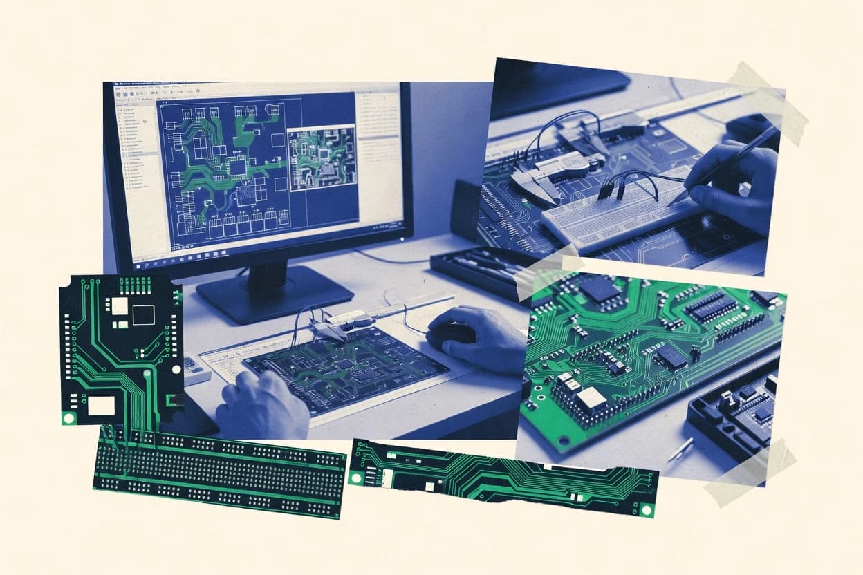
Manufacturing EngineeringTop 10 Best Circuit Design Software of 2026
Compare top Circuit Design Software picks for PCB and schematic work, including Altium Designer, KiCad, and Mentor PADS.

How we ranked these tools
Core product claims cross-referenced against official documentation, changelogs, and independent technical reviews.
Analyzed video reviews and hundreds of written evaluations to capture real-world user experiences with each tool.
AI persona simulations modeled how different user types would experience each tool across common use cases and workflows.
Final rankings reviewed and approved by our editorial team with authority to override AI-generated scores based on domain expertise.
Score: Features 40% · Ease 30% · Value 30%
Gitnux may earn a commission through links on this page — this does not influence rankings. Editorial policy
Editor’s top 3 picks
Three quick recommendations before you dive into the full comparison below — each one leads on a different dimension.
Altium Designer
Smart routing with design-rule and constraint awareness for high-speed PCB layouts
Built for teams needing top-tier PCB layout, constraint control, and electronics workflow integration.
KiCad
Editor pickInteractive design rule checking with ERC and DRC integrated into the editing workflow
Built for open-source-first circuit designers needing strong PCB checks and standard manufacturing outputs.
Mentor PADS
Editor pickDesign rule and constraint management tightly coupled to routing and layout checks
Built for pCB teams needing schematic-driven layout productivity and rule-based routing.
Related reading
Comparison Table
This comparison table ranks circuit design software used for schematic capture, PCB layout, and design verification across multiple workflows. It contrasts widely adopted tools such as Altium Designer, KiCad, Mentor PADS, Cadence OrCAD, and Autodesk EAGLE on capabilities, file and library compatibility, and typical use cases for small designs and complex industry projects.
Altium Designer
enterprise-suiteAltium Designer provides schematic capture and PCB layout with simulation-oriented workflows and manufacturer-ready output for electronic circuit design.
Smart routing with design-rule and constraint awareness for high-speed PCB layouts
Altium Designer stands out for its tightly integrated schematic capture and PCB design in one continuous workflow with deep electronics design rule support. Core capabilities include advanced FPGA and high-speed design planning, simulation and constraint-driven routing, and robust component and library management. The platform also delivers collaborative design via project organization and versionable assets, while maintaining strong tooling for fabrication outputs through Gerber and fabrication package generation.
- +Single-project workflow tightly links schematic, layout, and rules enforcement
- +Powerful constraint-driven routing supports high-speed and controlled-impedance design
- +Strong manufacturing outputs via fabrication package generation and layer stack tooling
- –Large learning curve for advanced rules, templates, and workflow setup
- –Resource-intensive projects can strain performance on mid-range hardware
- –Tooling depth increases configuration time before first productive use
Best for: Teams needing top-tier PCB layout, constraint control, and electronics workflow integration
More related reading
KiCad
open-sourceKiCad delivers schematic capture, PCB layout, and design-rule checking with an active component and plugin ecosystem for circuit design.
Interactive design rule checking with ERC and DRC integrated into the editing workflow
KiCad stands out by providing an open-source workflow that spans schematic capture and PCB layout in one toolchain. It supports hierarchical schematics, interactive routing, and a rule-driven ERC plus DRC pipeline that catches many electrical and fabrication issues before output.
It also includes built-in viewers and export paths for manufacturing outputs like Gerber, drill files, and pick-and-place data. The software’s flexibility shows in reusable footprints and libraries, along with project-level settings that keep large boards consistent across revisions.
- +Integrated schematic and PCB layout keeps connectivity consistent across the design flow
- +Rule-based ERC and DRC help surface electrical and constraint issues early
- +Powerful library and footprint management supports reusable component workflows
- +Gerber and drill exports cover common manufacturing output needs
- –New users need time to learn workflows and coordinate system conventions
- –Large projects can feel slower during global updates and rule checks
- –Library quality depends heavily on footprint and symbol curation
Best for: Open-source-first circuit designers needing strong PCB checks and standard manufacturing outputs
Mentor PADS
manufacturingMentor PADS supports schematic and PCB design workflows used in manufacturing-focused electronics development.
Design rule and constraint management tightly coupled to routing and layout checks
Mentor PADS stands out for its long-established workflow for schematic capture and PCB layout in professional electronic design environments. It combines schematic-driven PCB design with robust constraint handling, enabling teams to manage clearances, routing rules, and fabrication-ready outputs.
PADS also supports signal integrity workflows through analysis integrations, which helps verify high-speed design requirements. Overall, it focuses on practical layout productivity for board-level circuit design rather than code-based or model-only approaches.
- +Schematic-to-PCB synchronization reduces orphan parts and mapping errors
- +Strong rule- and constraint-driven routing for manufacturable board layouts
- +High-speed oriented features support practical SI-driven design verification workflows
- –User interface complexity can slow onboarding for new layout designers
- –Advanced automation tools often require careful setup of design rules
- –Deep toolchain integration needs experienced configuration to avoid rework
Best for: PCB teams needing schematic-driven layout productivity and rule-based routing
Cadence OrCAD
enterprise-suiteCadence OrCAD provides schematic capture and PCB design tooling that supports fabrication workflows for circuit boards.
OrCAD Capture schematic capture with tight netlisting and design rule handoff
Cadence OrCAD stands out for its long-established OrCAD Capture schematic capture workflow paired with simulation and verification flows. It supports schematic-driven design with library management and project-based organization across typical PCB design stages. It integrates with PCB layout and analysis toolchains in the OrCAD ecosystem for netlisting, design reuse, and sign-off oriented checking.
- +Strong schematic capture workflows with robust netlisting support
- +Good library reuse and project structure for consistent design iterations
- +Practical integration with simulation and PCB toolchains for verification
- –Workflow can feel dated versus modern EDA user interfaces
- –Advanced automation requires careful setup of constraints and rules
- –Toolchain coupling can increase configuration friction across stages
Best for: Engineering teams needing stable schematic capture and verification pipelines
Autodesk EAGLE
prototypingAutodesk EAGLE enables schematic capture and PCB layout for designing and releasing circuit boards with standard CAM outputs.
EAGLE CAM export workflow for producing Gerbers and manufacturing outputs
Autodesk EAGLE stands out for its tight integration of schematic capture and PCB layout in a single, mature workflow. The tool supports component libraries, ERC and DRC checks, and board fabrication output via CAM export and Gerber generation.
It also offers scripting and automation through EAGLE scripts, plus ecosystem-style add-ons for device and library management. For many teams, it functions as an efficient iteration engine from schematic to manufacturable PCB artwork.
- +Schematic-to-PCB workflow with reliable ERC and DRC checks
- +Strong CAM output pipeline for Gerbers and fabrication documentation
- +Scripting enables repeatable design automation and custom rules
- –Less suited for very large, highly collaborative PCB projects
- –Advanced automation often requires learning EAGLE scripting patterns
- –Modern UX and performance can lag behind newer layout tools
Best for: Engineers iterating small to mid-complexity PCBs with automation needs
Synopsys NanoSim
simulationSynopsys NanoSim focuses on SPICE simulation for electronic circuits and semiconductor-oriented circuit verification work.
Corner-based parametric simulation and automated sweep orchestration for robust signoff-oriented analysis
Synopsys NanoSim stands out by combining circuit simulation with mixed-signal device models and automated design rule checking flows for nanoscale technologies. The core capabilities center on SPICE-class analysis for analog and mixed-signal circuits, including transient, AC, and noise analysis with hierarchical netlists.
NanoSim also supports optimization-oriented workflows such as parametric sweeps and scripted runs that help verify robustness across process corners and operating conditions. Integration with Synopsys design and signoff environments strengthens end-to-end convergence for custom IC teams targeting advanced nodes.
- +Strong SPICE-class analog and mixed-signal analysis for transient, AC, and noise
- +Reliable support for process and operating-condition variation using corner-driven flows
- +Hierarchical, automation-friendly simulation suitable for large custom blocks
- –Workflow complexity is high for teams expecting a lightweight circuit simulator
- –Model setup and convergence tuning can take significant expertise and time
- –GUI-driven debugging is limited compared with script-first workflows
Best for: Teams doing custom analog and mixed-signal verification for advanced-node ICs
Multisim
simulationMultisim offers schematic entry and circuit simulation with measurement-oriented workflows for electrical engineering verification.
Oscilloscope and probe views tightly linked to SPICE simulation waveforms
Multisim stands out for its integrated SPICE simulation workflow tightly coupled to schematic capture in a single design canvas. It supports component-level circuit building, analog and mixed-signal simulation, and instrument-style views like oscilloscopes and logic analyzers.
The tool emphasizes fast iteration with wiring, probing, and waveform inspection, which suits education and prototyping cycles. Limitations show up in larger, multi-sheet digital projects and in dependency on NI-centric extensions for advanced system-level workflows.
- +Integrated schematic capture with immediate SPICE simulation feedback
- +Instrument-style measurement views for oscilloscopes and logic analysis
- +Large component library and straightforward model management
- +Good workflow for analog prototyping and lab-style verification
- –Multi-sheet and large digital designs can feel cumbersome
- –System-level architecture modeling is weaker than specialized EDA stacks
- –Advanced automation depends on NI tooling and scripted patterns
Best for: Analog and mixed-signal prototyping with fast schematic-to-waveform iteration
EasyEDA
web-basedEasyEDA provides web-based schematic capture and PCB layout with library management for fast circuit design iterations.
SPICE simulation directly on EasyEDA schematics
EasyEDA stands out for browser-first circuit design with instant shareable web schematics. It supports schematic capture plus PCB layout, and it links parts libraries to generate boards from the same design source. The tool also offers SPICE simulation for electronics testing, and it includes autorouting and design-rule checking during PCB work.
- +Browser-based schematic and PCB workflow reduces setup friction for circuit iterations
- +Integrated SPICE simulation supports quick verification without exporting files
- +Large component library accelerates building schematics and deriving PCB footprints
- –Advanced PCB workflow can feel constrained compared with dedicated desktop CAD tools
- –Simulation results can require careful model selection for realistic behavior
- –Large multi-sheet projects can become slower to navigate and manage
Best for: Prototyping engineers who want web schematics, simulation, and PCB output in one tool
JLCPCB EDA
fab-integratedJLCPCB EDA supports PCB layout and manufacturing handoff workflows optimized for quick quotation and production submission.
Fabrication data export tailored for PCB manufacturing file generation
JLCPCB EDA stands out for its tight connection to manufacturing-focused workflows and board turnaround operations. The tool provides schematic capture and PCB layout with board-level design checks aimed at producing fabrication-ready output.
It also supports generating manufacturing outputs from EDA data, including drill and fabrication documentation. The strongest fit is projects that want a streamlined path from design entry to production files rather than deep, custom simulation or advanced library governance.
- +Fabrication-output generation maps directly to board production needs
- +Integrated design rule checking helps catch common PCB issues early
- +Schematic-to-layout workflow reduces coordination friction between stages
- –Advanced IC-level simulation and verification depth is limited
- –Library and symbol management tools feel basic compared with top-tier EDA suites
- –Large or highly complex projects can feel less optimized for scale
Best for: Teams needing fast PCB design-to-fabrication output with practical checks
Upverter
web-basedUpverter offers browser-based schematic and PCB design focused on fast circuit creation and collaboration.
Browser-based schematic-to-PCB design flow with shared project collaboration
Upverter stands out for letting teams design electronics with a web-based schematic and PCB workflow that stays browser-centric. It supports hierarchical design, simulation-ready netlists, and collaborative revision handling for hardware projects.
The tool also provides library and footprint management aimed at accelerating layout and manufacturing preparation. Strong integration between schematic capture and board creation makes it practical for iterative circuit development.
- +Browser-based schematic to PCB workflow reduces context switching
- +Hierarchical design supports larger projects without flattening everything
- +Parts and footprints management speeds repeatable layout work
- –Advanced PCB constraints and detailed routing controls lag behind desktop CAD
- –Library gaps can require extra cleanup before layout readiness
- –Simulation depth is limited compared with dedicated EDA suites
Best for: Teams needing browser-first schematic and PCB design for iterative electronics
How to Choose the Right Circuit Design Software
This buyer’s guide explains how to pick circuit design software for schematic capture, PCB layout, simulation, and fabrication handoff. It covers Altium Designer, KiCad, Mentor PADS, Cadence OrCAD, Autodesk EAGLE, Synopsys NanoSim, Multisim, EasyEDA, JLCPCB EDA, and Upverter. Each tool is mapped to the real workflow strengths and constraints that drive successful circuit-to-boards or circuit verification outcomes.
What Is Circuit Design Software?
Circuit design software covers schematic entry, electrical checking, PCB layout, and often simulation or manufacturing export. These tools solve connectivity correctness, routing constraint compliance, and production-ready output problems. Teams use them to transform circuit intent into layout artwork, fabrication packages, and verification waveforms. Altium Designer and KiCad illustrate how one toolchain can span schematic capture through PCB DRC and output generation.
Key Features to Look For
The right feature set prevents late rework by catching electrical and manufacturing issues earlier and by matching the toolchain depth to the design workload.
Tightly integrated schematic-to-PCB workflow
Tools that keep schematic connectivity consistent through PCB editing reduce orphan parts and mapping errors during board updates. Altium Designer links schematic, layout, and constraint-aware routing in a single project workflow. Mentor PADS uses schematic-to-PCB synchronization to reduce coordination friction between stages.
Design-rule checking and constraint-driven routing
Strong rule engines enforce electrical and fabrication constraints during layout, not after the fact. KiCad integrates ERC and DRC into the editing workflow with interactive rule checking that surfaces issues early. Altium Designer supports constraint-driven routing for high-speed and controlled-impedance design.
Manufacturing-ready fabrication output generation
Good fabrication outputs convert layout intent into deliverables like Gerbers, drill files, and pick-and-place data. Autodesk EAGLE emphasizes CAM export workflows for producing Gerbers and fabrication documentation. EasyEDA and KiCad provide standard manufacturing exports like Gerber and drill outputs.
Simulation depth matched to circuit intent
Simulation tools should match analog or mixed-signal verification needs and the level of model sophistication required. Synopsys NanoSim focuses on SPICE-class analog and mixed-signal analysis with transient, AC, and noise using corner-based parametric sweeps. Multisim provides fast schematic-to-waveform iteration with instrument-style oscilloscopes and logic analysis views.
Hierarchical design and project collaboration support
Scalable project structure helps teams manage complex schematics and board revisions without flattening everything. Upverter supports hierarchical design plus browser-based collaborative revision handling. KiCad supports hierarchical schematics and keeps large boards consistent with project-level settings.
Library and footprint management quality
Reusable symbols and footprints reduce setup time and prevent functional errors from poor part data. Altium Designer provides robust component and library management tied to a fabrication-ready workflow. KiCad and EasyEDA both rely on footprint and symbol curation and can slow down when library quality is inconsistent.
How to Choose the Right Circuit Design Software
Selection should start with the required workflow depth and output targets, then match simulation and collaboration needs to the specific toolchain strengths.
Start with the dominant task: layout, verification, or both
Altium Designer and Mentor PADS fit teams whose primary work is schematic capture through PCB routing and manufacturable board generation. Synopsys NanoSim fits teams doing custom analog and mixed-signal verification for advanced-node IC work with transient, AC, and noise analysis. Multisim fits prototyping teams that need instrument-style oscilloscope and probe views tightly linked to SPICE waveforms.
Choose the rule checking style that matches the risk profile
KiCad offers interactive ERC and DRC integrated into the editing workflow, which helps catch electrical and constraint issues early for board correctness. Altium Designer excels when constraint-aware and design-rule-aware routing must support high-speed and controlled-impedance outcomes. Mentor PADS couples design-rule and constraint management tightly to routing and layout checks for manufacturable board layouts.
Confirm the fabrication outputs used by the manufacturing workflow
Autodesk EAGLE emphasizes CAM export workflows for producing Gerbers and fabrication documentation that many release processes already expect. JLCPCB EDA focuses on fabrication-output generation aimed at quick quotation and production submission, including drill and fabrication documentation. KiCad and EasyEDA cover common outputs like Gerber and drill files so PCB handoff remains predictable.
Match the collaboration and scale needs to project structure
Upverter supports browser-based schematic-to-PCB collaboration and hierarchical design, which is useful for teams that iterate together without desktop-only context switching. KiCad keeps large boards consistent across revisions using project-level settings and supports hierarchical schematics for scalability. EasyEDA supports browser-first schematic sharing, but navigation and multi-sheet handling can slow down for large projects.
Pick the level of automation expertise the team can support
Altium Designer and Mentor PADS offer deep tooling that requires configuration time for advanced rules, which can slow initial setup on new teams. Autodesk EAGLE provides scripting for repeatable automation but requires learning EAGLE scripting patterns for advanced workflows. Cadence OrCAD delivers stable schematic capture and netlisting for verification pipelines, but advanced automation needs careful setup of constraints and rules.
Who Needs Circuit Design Software?
Circuit design software serves teams ranging from analog prototypers to PCB manufacturing workflows and custom IC verification groups.
High-speed PCB teams that need constraint-aware routing and strong fabrication outputs
Altium Designer suits teams that need smart routing with design-rule and constraint awareness for high-speed PCB layouts and reliable fabrication package generation. Mentor PADS fits teams that prioritize schematic-to-PCB synchronization and tightly coupled rule and constraint management during routing and layout checks.
Open-source-first designers who want integrated electrical and manufacturing checks with standard outputs
KiCad fits open-source-first circuit designers who want ERC and DRC integrated into the editing workflow plus Gerber and drill exports. EasyEDA is a strong fit when the workflow must stay browser-first while still supporting schematic, PCB layout, and SPICE simulation.
Verification-focused engineers working on custom analog and mixed-signal blocks
Synopsys NanoSim fits teams that require SPICE-class analog and mixed-signal analysis across transient, AC, and noise with corner-driven parametric sweeps. Multisim fits teams that need fast schematic-to-waveform iteration with oscilloscope and probe views linked to SPICE simulation waveforms.
Teams that prioritize production file generation and fast board turnaround
JLCPCB EDA fits teams that want a streamlined design-to-production path with fabrication-data export tailored to PCB manufacturing file generation. Upverter fits teams that want a browser-based schematic-to-PCB workflow with hierarchical design and shared project collaboration for iterative electronics work.
Common Mistakes to Avoid
Frequent failures come from mismatching tool depth to the workflow stage, underestimating configuration effort, or choosing a simulation depth that cannot support the required circuit verification scope.
Choosing a deep rule and constraint workflow without planning for setup time
Altium Designer and Mentor PADS both have advanced tooling depth that increases configuration time before first productive use. KiCad also has workflow conventions that can require time to learn, especially for users who need consistent system conventions across projects.
Assuming a layout tool can deliver IC-class signoff simulation
EasyEDA and Upverter include SPICE simulation, but simulation depth is limited compared with dedicated EDA simulation stacks. Synopsys NanoSim is built for corner-based parametric simulation and automated sweep orchestration for robust signoff-oriented analysis.
Ignoring library and footprint data quality until late layout
KiCad and EasyEDA depend heavily on footprint and symbol curation, and poor library quality can slow down board readiness. Altium Designer’s robust component and library management reduces friction, while JLCPCB EDA provides basic symbol management that may require extra cleanup for advanced designs.
Optimizing for collaboration or iteration and then hitting constraint and routing limits
Upverter and EasyEDA are strong for browser-first schematic-to-PCB iteration, but advanced PCB constraints and detailed routing controls can lag behind desktop CAD tools. Altium Designer and Mentor PADS are better choices when constraint-driven routing control must match high-speed or tightly specified fabrication needs.
How We Selected and Ranked These Tools
we evaluated every tool on three sub-dimensions with weights of features at 0.40, ease of use at 0.30, and value at 0.30. The overall rating is the weighted average of those three scores using overall = 0.40 × features + 0.30 × ease of use + 0.30 × value. Altium Designer separated from lower-ranked tools on features by combining constraint-driven smart routing with a tightly integrated schematic-to-PCB workflow and manufacturing-focused fabrication package generation.
Frequently Asked Questions About Circuit Design Software
Which circuit design software keeps schematic capture and PCB layout tightly connected in one workflow?
What toolchain is best when open-source EDA workflows and built-in design rule verification matter most?
Which software is strongest for rule-controlled high-speed PCB routing and constraint handling?
Which option fits teams that need stable schematic capture plus simulation and verification sign-off workflows?
Which software is most suitable for advanced analog and mixed-signal verification using SPICE-class analysis and corners?
What tool is best for fast schematic-to-waveform iteration during prototyping and education?
Which browser-first tools help teams collaborate on schematics and produce PCB artifacts from shared projects?
Which software is focused on turning EDA data into fabrication outputs with practical manufacturability checks?
Which option is best when automated sweeps and scripted analysis runs are required for robustness testing?
Conclusion
After evaluating 10 manufacturing engineering, Altium Designer stands out as our overall top pick — it scored highest across our combined criteria of features, ease of use, and value, which is why it sits at #1 in the rankings above.
Use the comparison table and detailed reviews above to validate the fit against your own requirements before committing to a tool.
Tools reviewed
Primary sources checked during evaluation.
Referenced in the comparison table and product reviews above.
Keep exploring
Comparing two specific tools?
Software Alternatives
See head-to-head software comparisons with feature breakdowns, pricing, and our recommendation for each use case.
Explore software alternatives→In this category
Manufacturing Engineering alternatives
See side-by-side comparisons of manufacturing engineering tools and pick the right one for your stack.
Compare manufacturing engineering tools→FOR SOFTWARE VENDORS
Not on this list? Let’s fix that.
Our best-of pages are how many teams discover and compare tools in this space. If you think your product belongs in this lineup, we’d like to hear from you—we’ll walk you through fit and what an editorial entry looks like.
Apply for a ListingWHAT THIS INCLUDES
Where buyers compare
Readers come to these pages to shortlist software—your product shows up in that moment, not in a random sidebar.
Editorial write-up
We describe your product in our own words and check the facts before anything goes live.
On-page brand presence
You appear in the roundup the same way as other tools we cover: name, positioning, and a clear next step for readers who want to learn more.
Kept up to date
We refresh lists on a regular rhythm so the category page stays useful as products and pricing change.