GITNUXSOFTWARE ADVICE
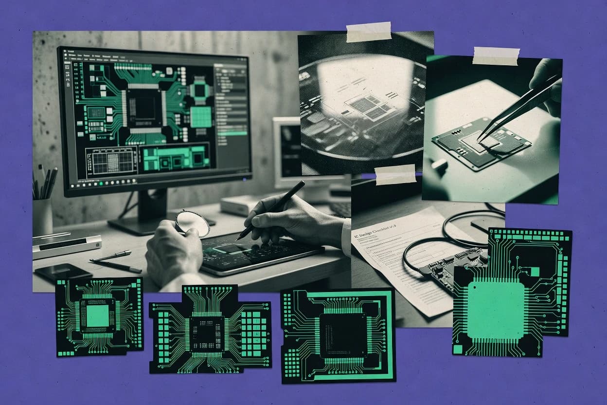
Manufacturing EngineeringTop 10 Best Chip Designing Software of 2026
Compare top 10 Chip Designing Software tools for fast custom IC design workflows, including Calibre and HSPICE. Explore the ranked picks.

How we ranked these tools
Core product claims cross-referenced against official documentation, changelogs, and independent technical reviews.
Analyzed video reviews and hundreds of written evaluations to capture real-world user experiences with each tool.
AI persona simulations modeled how different user types would experience each tool across common use cases and workflows.
Final rankings reviewed and approved by our editorial team with authority to override AI-generated scores based on domain expertise.
Score: Features 40% · Ease 30% · Value 30%
Gitnux may earn a commission through links on this page — this does not influence rankings. Editorial policy
Editor’s top 3 picks
Three quick recommendations before you dive into the full comparison below — each one leads on a different dimension.
Siemens EDA Calibre
Calibre PERC fault-oriented verification for DFM signoff using extracted physical intelligence
Built for large chip teams needing signoff-ready physical verification and signoff-quality reports.
Synopsys Custom Compiler
Editor pickCustom Compiler’s automation-driven physical implementation flow for connectivity-preserving custom design closure
Built for teams running Synopsys-centric custom and mixed-signal flows needing design closure automation.
Synopsys HSPICE
Editor pickMeasurement-based scripting with automated parametric sweeps across corners
Built for large teams needing signoff-grade transistor simulation and automated characterization.
Related reading
Comparison Table
This comparison table contrasts chip design and verification tools across layout, physical design, and simulation workflows. It covers Siemens EDA Calibre, Synopsys Custom Compiler, Synopsys HSPICE, Cadence Virtuoso, Cadence Allegro, and other widely used EDA platforms, focusing on what each tool is built to do. Readers can use the table to map specific tasks like custom layout, parasitic extraction, and circuit simulation to the most relevant software.
Siemens EDA Calibre
physical verificationCalibre performs physical verification for chip designs by checking layout against manufacturing rules and design intent.
Calibre PERC fault-oriented verification for DFM signoff using extracted physical intelligence
Siemens EDA Calibre stands out for verification-grade physical design signoff that targets manufacturability before tapeout. It combines rule-driven layout checking, analysis, and extraction for wafers and hierarchical designs.
Strong defect and reliability workflows integrate well with foundry and fabrication constraints across multiple process nodes. The tool emphasizes accuracy and traceability through detailed reporting tied to layout intent and PDK rules.
- +Highly accurate signoff physical verification with PDK-aligned rule sets
- +Efficient handling of large hierarchical layouts with targeted checks
- +Powerful defect-based analysis workflows linked to manufacturability constraints
- +Strong DRC and LVS coverage supports consistent tapeout readiness
- +Detailed reporting improves debug turnaround for physical issues
- –Setup and constraint management require experienced verification flows
- –Workflow customization can feel heavy for small design teams
- –Interpreting rule coverage and tolerances can take tuning time
- –Integration requires careful environment and run-script consistency
- –License and compute planning can constrain iterative usage patterns
Best for: Large chip teams needing signoff-ready physical verification and signoff-quality reports
More related reading
Synopsys Custom Compiler
custom IC automationCustom Compiler automates custom IC layout generation and optimization for analog, mixed-signal, and custom digital blocks.
Custom Compiler’s automation-driven physical implementation flow for connectivity-preserving custom design closure
Synopsys Custom Compiler is distinct for accelerating custom and mixed-signal chip flows through automation around schematic, layout, verification, and signoff-ready tasks. The tool supports custom layout and physical implementation workflows with connectivity awareness, enabling tight correlation between circuit intent and geometry.
It also integrates standard design closure capabilities for timing, power, and rule compliance so teams can iterate quickly from early builds to final verification. Strong results typically come from running it as part of an established Synopsys custom design stack rather than as a standalone utility.
- +Tight integration across custom implementation and verification reduces handoffs
- +Automation-oriented flow support helps teams iterate on layout and closure
- +Connectivity-aware physical workflows improve consistency from schematic to layout
- –Best performance depends on established Synopsys toolchain and flow discipline
- –Setup and scripting effort can be high for nonstandard process targets
- –Debugging complex flow failures often requires specialized physical design knowledge
Best for: Teams running Synopsys-centric custom and mixed-signal flows needing design closure automation
Synopsys HSPICE
circuit simulationHSPICE simulates chip circuits with device-level accuracy for verification of performance, power, noise, and timing.
Measurement-based scripting with automated parametric sweeps across corners
Synopsys HSPICE stands out for high-fidelity circuit simulation driven by an established SPICE engine used in production IC design flows. It supports detailed transistor-level analysis for large and mixed-signal designs, including transient, DC operating point, AC, noise, and parametric sweeps.
Strong integration supports hierarchical netlists and industry-standard device and model handling used for signoff-style verification. The tool also offers advanced measurement and scripting workflows to automate characterization across corners and scenarios.
- +High-accuracy SPICE simulation for transistor-level verification
- +Robust support for mixed-signal and hierarchical netlists
- +Strong parametric sweeps with measurement-driven automation
- +Mature modeling and device support for production design flows
- +Efficient handling of large operating-point and transient workloads
- –Steeper learning curve due to SPICE deck and measurement syntax
- –Run setup and debug can take significant iteration for complex cases
- –Workflow efficiency depends on external scripting and flow integration
- –Less oriented to exploratory UI-driven analysis than some simulators
- –Tuning convergence and sources for difficult circuits needs expertise
Best for: Large teams needing signoff-grade transistor simulation and automated characterization
More related reading
Cadence Virtuoso
custom design suiteVirtuoso supports schematic capture, custom layout, and signoff-ready verification flows for IC design.
DRC and LVS verification tightly coupled to Virtuoso physical design.
Cadence Virtuoso is distinguished by its long-standing, tapeout-ready EDA workflow for custom IC design and signoff. It supports schematic capture, hierarchical layout, and extensive custom layout editing with DRC and LVS checks.
The environment also integrates parasitic-aware simulation and verification flows that connect design intent to physical implementation. Its strength is controlling complex analog and custom digital blocks inside a single, tightly integrated toolchain.
- +End-to-end custom IC flow from schematic to verified layout.
- +Powerful DRC and LVS capabilities for tapeout readiness.
- +Strong hierarchy and layout editing support for complex blocks.
- +Tight integration with simulation and parasitic extraction flows.
- +Mature environment with deep IP and methodology compatibility.
- –Toolchain complexity requires specialized training and process discipline.
- –Interactive performance can suffer on very large hierarchical designs.
- –Workflow setup for PDKs and signoff checks can be labor intensive.
Best for: Analog-heavy IC teams needing signoff-grade custom layout verification
Cadence Allegro
interconnect layoutAllegro enables PCB and high-density interconnect layout and analysis to support manufacturable chip package and board design handoffs.
Constraint manager-driven design rule enforcement during interactive and automated routing
Cadence Allegro targets full chip and PCB implementation with deep EDA integration across capture, simulation, and signoff flows. It is known for constraint-driven layout, advanced routing, and robust physical verification support for complex, high-density designs. The tool excels when strict manufacturing rules, signal integrity needs, and large design reuse require repeatable implementation control.
- +Constraint-driven placement and routing supports complex rule sets
- +Powerful physical verification and DRC coverage for high-density designs
- +Scales to large layouts with efficient interactive editing workflows
- –Steep learning curve for automation, constraints, and methodology setup
- –Workflow overhead increases for teams without established signoff standards
- –Customization and scripting require strong EDA process discipline
Best for: Large teams needing rule-driven PCB implementation and rigorous physical verification
Cadence Virtuoso Spectre
circuit simulationSpectre provides circuit simulation for custom ICs and system-level verification with advanced modeling support.
Advanced convergence and accuracy controls for reliable mixed-signal simulation
Cadence Virtuoso Spectre stands out for fast, accurate circuit simulation built for industrial design flows. It supports mixed-signal, device-level analog, and system-level verification using SPICE-based modeling and advanced numerical methods.
Designers rely on it for signal integrity analysis and timing-aware verification across complex IC test and characterization tasks. Tight integration with the Virtuoso environment helps streamline netlisting, re-simulation, and debug between schematic and verification.
- +High-fidelity analog and mixed-signal simulation with robust convergence aids
- +Strong support for signal integrity style analyses and extraction-driven verification
- +Tight schematic to verification integration reduces manual netlisting effort
- –Steep setup learning curve for advanced convergence and accuracy controls
- –Large simulations can require significant tuning to keep runtimes manageable
- –Debugging obscure convergence issues often demands deep simulator expertise
Best for: Analog and mixed-signal IC teams needing high-accuracy Spectre verification
More related reading
Zuken CR-8000
PCB CAD suitePerforms electronic CAD design, board-level engineering, and constraint-driven signal and design-rule checks for manufacturing-ready PCB layouts.
Hierarchical chip design data management with object-level traceability across revisions
Zuken CR-8000 stands out as an EDA workbench focused on chip and IC design data management with strong cross-domain connectivity into electronic CAD workflows. The core capabilities center on hierarchical design handling, schematic-driven data organization, and structured support for chip assembly views used during electronics-to-chip development handoffs.
It also emphasizes traceability between design objects so teams can manage revisions across complex component and interface definitions. The result is a configuration-centric approach that fits engineering processes built around controlled design repositories and consistent naming conventions.
- +Strong hierarchical design management for chip-level organization and reuse
- +Good traceability between design objects across revision cycles
- +Well-aligned with engineering workflows that need consistent naming and structure
- –Steeper learning curve for teams unfamiliar with structured chip design data models
- –Less suited for quick exploratory layout work compared with layout-first tools
- –Workflow setup and data governance require disciplined process adoption
Best for: Teams managing chip design data handoffs with controlled structure
Altium Designer
PCB designSupports schematic capture, PCB layout, and manufacturing output generation with a focus on high-density board design workflows.
Constraint-driven design rule checking with automated schematic-to-PCB synchronization
Altium Designer stands out for deep, constraint-driven PCB and chip-focused design workflows backed by an integrated rules system. It supports hierarchical design reuse, powerful parametric footprint management, and board-level to fabrication-ready outputs in one environment.
Large-project collaboration features connect schematics, PCB layout, and library data into a single verification loop that reduces mismatch risk between chip symbols, footprints, and packages. Advanced connectivity checking and DRC-style enforcement make it strong for high-density designs that require tight control of net integrity and manufacturing constraints.
- +Constraint-driven DRC enforces net, footprint, and manufacturing rules throughout design
- +Library and parametric component management keeps chip footprints consistent across projects
- +Tight schematic-to-layout integration reduces symbol and package mismatches
- +High-density layout tools support precise routing, plane modeling, and stackup control
- +Built-in verification workflows streamline connectivity, design-rule, and manufacturability checks
- –Learning curve is steep due to many advanced panels, rules, and editor modes
- –Performance can degrade on very large boards with complex connectivity and rule sets
- –Library customization takes time to set up and maintain across multiple component versions
Best for: Teams building high-density PCBs requiring strong chip-package consistency and verification
More related reading
Autodesk EAGLE
PCB CADProvides schematic and PCB layout design tools that generate fabrication files for electronics manufacturing.
Design Rule Check with netlist-linked schematic and board synchronization
Autodesk EAGLE stands out with a fast, file-based PCB workflow built around schematic capture tied directly to board layout. It supports hierarchical schematics, ERC checks, and rule-driven PCB design including footprints, netlists, and design-rule checking.
The library model and Cam processor enable repeatable outputs such as Gerber layers, drill files, and manufacturing documentation from a single project structure. Tight integration with Autodesk tooling makes EAGLE practical for board-level design rather than deep semiconductor device simulation.
- +Schematic-to-layout synchronization reduces netlist errors during board iteration
- +Design-rule checking enforces clear constraints across routing, spacing, and layers
- +Solid Gerber and drill export pipeline supports common manufacturing workflows
- –EAGLE focuses on PCB design, not chip-level physical design automation
- –Large design performance can degrade when projects grow and libraries are heavy
- –Advanced constraint and DFM flows require careful setup and external tooling
Best for: Teams designing PCBs from schematics needing rule-based layout and reliable exports
KiCad
open-source PCB CADOffers an open-source ECAD toolchain for schematic capture and PCB layout with design-rule checking and fabrication output generation.
Design rule checker enforcing clearance and routing constraints during PCB layout
KiCad stands out for being a full, open-source electronics design suite that covers schematic capture, PCB layout, and fabrication outputs in one workflow. It supports chip-oriented design tasks through symbol and footprint libraries, hierarchical schematics, and constraint-driven annotation to keep netlists consistent.
Users can generate manufacturing deliverables such as Gerbers, drilling files, and bill-of-materials data directly from the same project. Tooling also includes design rule checking and 2D drafting capabilities that fit iterative board and component refinement cycles.
- +Integrated schematic, PCB, and manufacturing output generation from one project
- +Strong footprint and symbol library workflow with custom library support
- +Design rule checking catches clearance and constraint issues before export
- +Hierarchical schematics and net annotation help maintain consistency
- –3D visualization and some advanced placement tools are less streamlined than premium suites
- –Complex design workflows can feel slower to navigate and configure
- –BOM and variant management require more manual setup for large projects
- –Advanced constraints and automation features lag behind specialized EDA platforms
Best for: Teams needing open ECAD for chip-centric PCB design and fabrication exports
How to Choose the Right Chip Designing Software
This buyer’s guide helps teams choose chip designing software by mapping tool capabilities to tapeout workflows across Siemens EDA Calibre, Synopsys Custom Compiler, Synopsys HSPICE, Cadence Virtuoso, and Cadence Virtuoso Spectre. It also covers PCB and interconnect implementation tools like Cadence Allegro, plus chip data management like Zuken CR-8000. The guide uses concrete selection criteria drawn from how these tools handle verification, simulation, routing constraints, and design data traceability.
What Is Chip Designing Software?
Chip designing software is the EDA toolchain used to capture circuit intent, generate physical layouts, verify manufacturability, and run signoff-grade checks before tapeout. It also covers SPICE-level simulation and mixed-signal verification so circuit behavior matches the implemented geometry. Large IC teams use tools like Cadence Virtuoso for schematic to custom layout signoff and Siemens EDA Calibre for physical verification that checks layout against manufacturing rules and design intent. Custom and mixed-signal teams often use Synopsys Custom Compiler to automate connectivity-aware custom implementation and closure steps.
Key Features to Look For
The right feature set determines whether a team can close design issues early, enforce manufacturability rules consistently, and keep simulation and verification loops reliable.
Signoff-grade physical verification aligned to PDK rules
Siemens EDA Calibre provides verification-grade physical signoff by checking layout against manufacturing rules and design intent with PDK-aligned rule sets. Calibre also produces defect-based analysis workflows and detailed reporting that improves debug turnaround for physical issues.
Connectivity-aware custom implementation automation
Synopsys Custom Compiler accelerates custom and mixed-signal chip flows by automating physical implementation around schematic, layout, verification, and signoff-ready tasks. Its connectivity-aware workflows support tight correlation between circuit intent and geometry during design closure.
Transistor-level simulation with measurement automation across corners
Synopsys HSPICE delivers high-fidelity SPICE simulation with device-level accuracy for performance, power, noise, and timing. It also supports measurement-based scripting and automated parametric sweeps across corners to speed characterization and signoff-style verification.
Tightly integrated custom layout verification with DRC and LVS
Cadence Virtuoso combines schematic capture, hierarchical layout editing, and tapeout-ready DRC and LVS checks in one environment. This tight coupling helps analog-heavy teams drive tapeout readiness directly from layout verification and parasitic-aware flows.
Mixed-signal simulation reliability controls for convergence and accuracy
Cadence Virtuoso Spectre is built for reliable analog and mixed-signal simulation with advanced convergence and accuracy controls. Spectre’s tighter integration with Virtuoso reduces manual netlisting effort between schematic and verification.
Constraint-driven rule enforcement across routing and design stages
Cadence Allegro enforces manufacturing rules through a constraint manager during interactive and automated routing for complex, high-density designs. Altium Designer and Autodesk EAGLE apply constraint-driven checking and DRC-style enforcement with schematic-to-layout synchronization to reduce mismatches between symbols, footprints, and manufacturing outputs.
How to Choose the Right Chip Designing Software
The selection framework starts by identifying whether the critical path is physical signoff, custom layout automation, transistor-level characterization, or constraint-driven board and interconnect implementation.
Match the tool to the design closure bottleneck
If manufacturability signoff and physical defect closure drive the schedule, Siemens EDA Calibre fits because it performs verification-grade physical checks tied to layout intent and PDK rules with strong defect and reliability workflows. If custom analog and mixed-signal implementation automation drives closure, Synopsys Custom Compiler fits because it automates connectivity-preserving physical implementation from schematic through signoff-ready tasks. If tapeout readiness depends on DRC and LVS verification within a single custom workflow, Cadence Virtuoso fits because its DRC and LVS are tightly coupled to Virtuoso physical design.
Plan for the simulation style and automation needs
Choose Synopsys HSPICE when transistor-level accuracy and measurement-driven automation across corners are required, since it supports DC, AC, noise, transient, and parametric sweeps with measurement scripting. Choose Cadence Virtuoso Spectre when mixed-signal verification needs advanced convergence and accuracy controls for reliable runtimes on complex test and characterization tasks.
Validate that physical checks connect to debug workflows
For physical issues tied to manufacturability, Siemens EDA Calibre stands out with detailed reporting that is linked to layout intent and PDK rules. For custom blocks that need verification tightly coupled to editing, Cadence Virtuoso provides DRC and LVS checks inside the same environment so layout fixes and verification feedback stay in one loop.
Use constraint enforcement tools when rule compliance is a routing problem
If complex high-density routing and strict manufacturing rules are the limiting factor, Cadence Allegro provides constraint-driven placement and routing with powerful physical verification and DRC coverage. If the design flow is board-focused with chip-package consistency needs, Altium Designer focuses on constraint-driven DRC with automated schematic-to-PCB synchronization so symbol and footprint mismatches are reduced.
Ensure the design data model supports handoffs and hierarchy
If chip assembly views, hierarchical organization, and revision traceability drive cross-team handoffs, Zuken CR-8000 supports hierarchical chip design data management with object-level traceability. If the workflow is schematic-to-board with fabrication export requirements, Autodesk EAGLE and KiCad support netlist-linked rule checking and generation of Gerber and drill outputs that keep design intent synchronized during board iteration.
Who Needs Chip Designing Software?
Chip designing software fits teams that must connect design intent to physical implementation, validate against manufacturing constraints, and run signoff-grade simulation and verification.
Large chip teams focused on tapeout-quality physical signoff
Siemens EDA Calibre fits large teams because it targets signoff-ready physical verification with PDK-aligned rule sets and efficient handling of large hierarchical layouts with targeted checks. The tool’s defect-based analysis and detailed reporting support reliable manufacturability closure before tapeout.
Custom IC teams and mixed-signal teams using Synopsys-centric flows
Synopsys Custom Compiler fits teams already operating within a Synopsys custom design stack because it automates custom layout generation and connectivity-preserving physical implementation. This tight integration reduces handoffs across schematic, layout, verification, and signoff-ready tasks.
Analog-heavy IC teams running custom layout verification loops
Cadence Virtuoso fits analog-heavy teams because it provides end-to-end custom IC flow from schematic to verified layout with DRC and LVS for tapeout readiness. It also supports hierarchy and extensive custom layout editing for complex blocks under one toolchain.
Mixed-signal design teams needing reliable simulation convergence controls
Cadence Virtuoso Spectre fits mixed-signal IC teams because it provides high-fidelity simulation with robust convergence aids and advanced convergence and accuracy controls. Its integration with Virtuoso streamlines netlisting and re-simulation between schematic and verification.
Common Mistakes to Avoid
Several recurring pitfalls appear across these tools when teams mismatch the tool to the closure task, underinvest in environment setup, or ignore workflow discipline for rule constraints.
Choosing a signoff-grade physical verification tool without allocating expertise to constraints
Siemens EDA Calibre delivers highly accurate signoff physical verification, but setup and constraint management require experienced verification flows. Tool adoption succeeds when run-script consistency and environment integration are treated as part of the verification plan rather than a late-stage task.
Running connectivity and closure automation without established flow discipline
Synopsys Custom Compiler provides automation-driven physical implementation, but best performance depends on established Synopsys toolchain and flow discipline. Debugging complex flow failures also requires specialized physical design knowledge for nonstandard process targets.
Using transistor simulation without preparing for SPICE deck learning and measurement syntax
Synopsys HSPICE is strong for production-grade transistor simulation, but SPICE deck and measurement syntax create a steeper learning curve. Teams reduce iteration time by investing early in run setup, convergence troubleshooting, and scripting workflows for automated parametric sweeps.
Treating routing constraints as optional when manufacturing rules are strict
Cadence Allegro and constraint-driven solutions like Altium Designer enforce rule compliance through constraint manager workflows and DRC-style enforcement during routing and design stages. Omitting constraint governance increases the risk of late rule failures and symbol or footprint mismatch errors in schematic-to-layout synchronization loops.
How We Selected and Ranked These Tools
We evaluated every tool on three sub-dimensions with weights of 0.4 for features, 0.3 for ease of use, and 0.3 for value, and computed overall as overall = 0.40 × features + 0.30 × ease of use + 0.30 × value. Siemens EDA Calibre separated itself because its features score reflected verification-grade physical signoff that checks layout against manufacturing rules and design intent with PDK-aligned rule sets and strong defect-based analysis tied to manufacturability constraints. That capability directly supports tapeout readiness with signoff-quality reports, which strengthens how features translate into practical closure speed compared with tools that focus more on data management, board routing, or simulation alone.
Frequently Asked Questions About Chip Designing Software
Which tool set fits teams that need physical design signoff and manufacturability checks?
How do Synopsys Custom Compiler and Cadence Virtuoso differ for custom and mixed-signal design closure?
Which simulator is best when transistor-level fidelity and automated corner characterization drive signoff workflows?
What option supports advanced analog block control when complex custom digital and analog must stay inside one environment?
Which software is more appropriate for full chip or high-density PCB routing under strict manufacturing rules?
When mixed-signal simulation speed and convergence control matter during debug, which tool is commonly used?
Which tool helps manage chip design data and trace revisions across hierarchical objects for engineering handoffs?
What is the best choice for preventing chip-package mismatches between schematic symbols and PCB footprints?
How do Altium Designer, Autodesk EAGLE, and KiCad compare when generating manufacturing deliverables from a single project workflow?
Conclusion
After evaluating 10 manufacturing engineering, Siemens EDA Calibre stands out as our overall top pick — it scored highest across our combined criteria of features, ease of use, and value, which is why it sits at #1 in the rankings above.
Use the comparison table and detailed reviews above to validate the fit against your own requirements before committing to a tool.
Tools reviewed
Primary sources checked during evaluation.
Referenced in the comparison table and product reviews above.
Keep exploring
Comparing two specific tools?
Software Alternatives
See head-to-head software comparisons with feature breakdowns, pricing, and our recommendation for each use case.
Explore software alternatives→In this category
Manufacturing Engineering alternatives
See side-by-side comparisons of manufacturing engineering tools and pick the right one for your stack.
Compare manufacturing engineering tools→FOR SOFTWARE VENDORS
Not on this list? Let’s fix that.
Our best-of pages are how many teams discover and compare tools in this space. If you think your product belongs in this lineup, we’d like to hear from you—we’ll walk you through fit and what an editorial entry looks like.
Apply for a ListingWHAT THIS INCLUDES
Where buyers compare
Readers come to these pages to shortlist software—your product shows up in that moment, not in a random sidebar.
Editorial write-up
We describe your product in our own words and check the facts before anything goes live.
On-page brand presence
You appear in the roundup the same way as other tools we cover: name, positioning, and a clear next step for readers who want to learn more.
Kept up to date
We refresh lists on a regular rhythm so the category page stays useful as products and pricing change.